
Datasheet
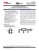


TPS71501-Q1
TPS71525-Q1, TPS71530-Q1
TPS71533-Q1, TPS71550-Q1
SGLS272G –OCTOBER 2004–REVISED JULY 2013
www.ti.com
This integrated circuit can be damaged by ESD. Texas Instruments recommends that all integrated circuits be handled with
appropriate precautions. Failure to observe proper handling and installation procedures can cause damage.
ESD damage can range from subtle performance degradation to complete device failure. Precision integrated circuits may be more
susceptible to damage because very small parametric changes could cause the device not to meet its published specifications.
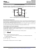
AVAILABLE OPTIONS
For the most current package and ordering information, see the Package Option Addendum at the end of this
document, or see the TI web site at www.ti.com.
Package drawings, thermal data, and symbolization are available at www.ti.com/packaging.
Contact Texas Instruments for other voltage options between 1.25 V and 5.85 V.
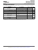
ABSOLUTE MAXIMUM RATINGS
over operating temperature range (unless otherwise noted)
(1) (2)
UNIT
V
IN
range –0.3 V to 24 V
V
OUT
range –0.3 V to 16.5 V
Peak output current Internally limited
ESD rating, HBM H2 2 kV
ESD rating, CDM C4B 750 V
Continuous total power dissipation See Dissipation Rating Table
Junction temperature range, T
J
–40°C to 150°C
Storage temperature range, T
stg
–65°C to 150°C
(1) Stresses beyond those listed under absolute maximum ratings may cause permanent damage to the device. These are stress ratings
only, and functional operation of the device at these or any other conditions beyond those indicated under recommended operating
conditions is not implied. Exposure to absolute-maximum-rated conditions for extended periods may affect device reliability.
(2) All voltage values are with respect to network ground terminal.
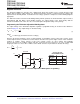
DISSIPATION RATING TABLE
DERATING FACTOR T
A
≤ 25°C T
A
= 70°C T
A
= 85°C
BOARD PACKAGE R
θJC
°C/W R
θJA
°C/W
ABOVE T
A
= 25°C POWER RATING POWER RATING POWER RATING
Low-K
(1)
DCK 165 395 2.52 mW/°C 250 mW 140 mW 100 mW
High-K
(2)
DCK 165 315 3.18 mW/°C 320 mW 175 mW 130 mW
(1) The JEDEC Low-K (1s) board design used to derive this data was a 3-in × 3-in, two-layer board with 2-oz copper traces on top of the
board.
(2) The JEDEC High-K (2s2p) board design used to derive this data was a 3-in × 3-in, multilayer board with 1-oz internal power and ground
planes and 2-oz copper traces on top and bottom of the board.
2 Submit Documentation Feedback Copyright © 2004–2013, Texas Instruments Incorporated
Product Folder Links: TPS71501-Q1 TPS71525-Q1 TPS71530-Q1 TPS71533-Q1 TPS71550-Q1