
User manual


www.ti.com
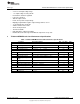
TPS65137AEVM Assembly Drawings and Layout
Figure 3. TPS65137A Software Window
Remove the jumper from the enable connector, JP1, to enable control of the EVM via the TPS65137A
software. On the left top corner is the 'Enable Device' button that turns the TPS65137A on with the default
-4.9 V on OUTN. After this button is pressed, it grays out and the 'Disable Device' button becomes active.
With the drop-down menus, the selections 'Pulse Off-Time' and 'Pulse On-Time' can be used to change
the pulse width of the controlling signal between 4 µs and 24 µs to test the different pulse widths possible
with this interface. For more details on the interface, see the TPS65137A data sheet.
On the right side, the list of possible output voltages is displayed. By clicking on one of the output
voltages, the software sends the necessary amount of rising edges to change the DAC value in the
TPS65137A, which finally changes the voltage on the negative rail, OUTN. Whenever the part is disabled
and enabled again, it starts with the default negative output voltage of -4.9 V.
6 TPS65137AEVM Assembly Drawings and Layout
Figure 4 through Figure 6 show the design of the TPS65137AEVM printed-circuit board (PCB). The EVM
has been designed using a two-layer, 35-mm (1 oz), copper-clad circuit board. All components are on the
top side, and all active traces on the top and bottom layers allow the user to easily view, probe, and
evaluate the TPS65137A control IC in a practical, double-sided application. Moving components to both
sides of the PCB or using additional internal layers can offer additional size reduction for
space-constrained systems.
7
SLVU378–August 2010 TPS65137A Evaluation Module
Copyright © 2010, Texas Instruments Incorporated