
User manual


5.9 TP1 – Test Point 1
5.10 TP2 – Test Point 2
6 Test Setup and Results
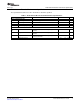
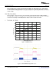
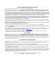
0
10
20
30
40
50
60
70
80
90
0 5 10 15 20 25
ILED-LEDCurrent-mA
LEDEfficiency-%
30
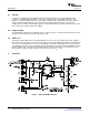
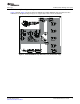
Time=200 s/divµ
ILED=20mV/div
IL =500mA/div
Vo-AC=100mV/div
Test Setup and Results
www.ti.com
This test point connects to the IC's VO pin. Since the VO pin is the output of the boost converter before
the internal PWM dimming switching, the user can monitor the boost converter output and, for example,
confirm that the over voltage protection circuit properly clamps the output voltage if the LEDs are removed
from the output.
This test point can be used to measure the small signal control loop gain and phase with Venable® or
similar gain phase analyzer. For example, the user would replace the 0- Ω resistor in R2 with a 49.9-100 Ω
resistor before attaching a Venable® gain/phase analyzer between header J5 and TP2.
Figure 2. LED Efficiency
Figure 3. 1kHz PWM Dimming with D = 30%
TPS61166EVM-446 User's Guide6 SLVU326 – October 2009
Submit Documentation Feedback