
Datasheet

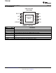

1
2
3
4
8
7
6
5
PowerPAD
(Pin9)
BOOT
NC
NC
VSENSE
PH
VIN
GND
ENA
DDAPACKAGE
(TOPVIEW)
TPS5450-Q1
SLVS834A –JULY 2008– REVISED OCTOBER 2011
www.ti.com
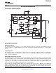
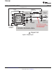
PIN ASSIGNMENTS
TERMINAL FUNCTIONS
TERMINAL
DESCRIPTION
NAME NO.
BOOT 1 Boost capacitor for the high-side FET gate driver. Connect 0.01-μF low-ESR capacitor from BOOT pin to PH pin.
NC 2, 3 No internal connection
VSENSE 4 Feedback voltage for the regulator. Connect to output voltage divider.
ENA 5 On/off control. Below 0.5 V, the device stops switching. Float the pin to enable.
GND 6 Ground. Connect to thermal pad.
Input supply voltage. Bypass VIN pin to GND pin close to device package with a high-quality low-ESR ceramic
VIN 7
capacitor.
PH 8 Source of the high side power MOSFET. Connected to external inductor and diode.
PowerPAD 9 GND pin must be connected to the exposed pad for proper operation.
4 Submit Documentation Feedback Copyright © 2008–2011, Texas Instruments Incorporated
Product Folder Link(s): TPS5450-Q1