
Datasheet


TPS5450-Q1
www.ti.com
SLVS834A –JULY 2008– REVISED OCTOBER 2011
DISSIPATION RATINGS
(1) (2)
THERMAL IMPEDANCE
PACKAGE
JUNCTION-TO-AMBIENT
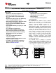
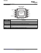
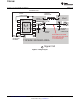
8-Pin DDA (4-layer board with solder)
(3)
30°C/W
(1) Maximum power dissipation may be limited by overcurrent protection.
(2) Power rating at a specific ambient temperature T
A
should be determined with a junction temperature of 125°C. This is the point where
distortion starts to substantially increase. Thermal management of the final PCB should strive to keep the junction temperature at or
below 125°C for best performance and long-term reliability. See Thermal Calculations in applications section of this data sheet for more
information.
(3) Test board conditions:
(a) 2 in x 1.85 in, 4 layers, 0.062-in (1,57-mm) thickness
(b) 2-oz copper traces located on the top and bottom of the PCB
(c) 2-oz copper ground planes on the two internal layers
(d) Four thermal vias in the PowerPAD area under the device package
RECOMMENDED OPERATING CONDITIONS
MIN MAX UNIT
V
I
Input voltage range 5.5 36 V
T
J
Operating virtual-junction temperature –40 125 °C
ELECTRICAL CHARACTERISTICS
T
J
= –40°C to 125°C, VIN = 5.5 V to 36 V (unless otherwise noted)
PARAMETER TEST CONDITIONS MIN TYP MAX UNIT
SUPPLY VOLTAGE (VIN PIN)
VSENSE = 2 V, Not switching, PH pin open 3 4.4 mA
I
Q
Quiescent current
Shutdown, ENA = 0 V 18 50 μA
UNDERVOLTAGE LOCK OUT (UVLO)
Start threshold voltage, UVLO 5.3 5.5 V
Hysteresis voltage, UVLO 330 mV
VOLTAGE REFERENCE
T
J
= 25°C 1.202 1.221 1.239
Voltage reference accuracy V
I
O
= 0 A – 5 A 1.196 1.221 1.245
OSCILLATOR
Internally set free-running frequency 400 500 600 kHz
Minimum controllable on time 150 200 ns
Maximum duty cycle 87 89 %
ENABLE (ENA PIN)
Start threshold voltage, ENA 1.3 V
Stop threshold voltage, ENA 0.5 V
Hysteresis voltage, ENA 450 mV
Internal slow-start time (0~100%) 5.4 8 10 ms
CURRENT LIMIT
Current limit 5.7 7.5 9.0 A
Current limit hiccup time 13 16 21 ms
THERMAL SHUTDOWN
Thermal shutdown trip point 135 162 °C
Thermal shutdown hysteresis 14 °C
OUTPUT MOSFET
VIN = 5.5 V 150
r
DS(on)
High-side power MOSFET switch mΩ
110 230
Copyright © 2008–2011, Texas Instruments Incorporated Submit Documentation Feedback 3
Product Folder Link(s): TPS5450-Q1