
Datasheet


TPS5450-Q1
SLVS834A –JULY 2008– REVISED OCTOBER 2011
www.ti.com
This integrated circuit can be damaged by ESD. Texas Instruments recommends that all integrated circuits be handled with
appropriate precautions. Failure to observe proper handling and installation procedures can cause damage.
ESD damage can range from subtle performance degradation to complete device failure. Precision integrated circuits may be more
susceptible to damage because very small parametric changes could cause the device not to meet its published specifications.
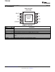
ORDERING INFORMATION
(1)
T
J
PACKAGE
(2)
ORDERABLE PART NUMBER TOP-SIDE MARKING
Thermally Enhanced
–40°C to 125°C Reel of 2500 TPS5450QDDARQ1 5450Q
SOIC – DDA
(1) For the most current package and ordering information, see the Package Option Addendum at the end of this document, or see the TI
web site at www.ti.com.
(2) Package drawings, thermal data, and symbolization are available at www.ti.com/packaging.
ABSOLUTE MAXIMUM RATINGS
over operating free-air temperature range (unless otherwise noted)
(1) (2)
VIN –0.3 V to 40 V
(3)
BOOT –0.3 V to 50 V
PH (steady-state) –0.6 V to 40 V
(3)
V
I
Input voltage range ENA –0.3 V to 7 V
BOOT-PH 10 V
VSENSE –0.3 V to 3 V
PH (transient < 10 ns) –1.2 V
I
O
Source current PH Internally Limited
I
lkg
Leakage current PH 10 μA
T
J
Operating virtual-junction temperature range –40°C to 150°C
T
stg
Storage temperature –65°C to 150°C
(1) Stresses beyond those listed under absolute maximum ratings may cause permanent damage to the device. These are stress ratings
only and functional operation of the device at these or any other conditions beyond those indicated under recommended operating
conditions is not implied. Exposure to absolute-maximum-rated conditions for extended periods may affect device reliability.
(2) All voltage values are with respect to network ground terminal.
(3) Approaching the absolute maximum rating for the VIN pin may cause the voltage on the PH pin to exceed the absolute maximum rating.
THERMAL INFORMATION
TPS5450-Q1
THERMAL METRIC
(1)
DDA UNITS
8 PINS
θ
JA
Junction-to-ambient thermal resistance
(2)
48.2
θ
JCtop
Junction-to-case (top) thermal resistance
(3)
47.1
θ
JB
Junction-to-board thermal resistance
(4)
22.5
°C/W
ψ
JT
Junction-to-top characterization parameter
(5)
5.4
ψ
JB
Junction-to-board characterization parameter
(6)
22.4
θ
JCbot
Junction-to-case (bottom) thermal resistance
(7)
2.9
(1) For more information about traditional and new thermal metrics, see the IC Package Thermal Metrics application report, SPRA953.
(2) The junction-to-ambient thermal resistance under natural convection is obtained in a simulation on a JEDEC-standard, high-K board, as
specified in JESD51-7, in an environment described in JESD51-2a.
(3) The junction-to-case (top) thermal resistance is obtained by simulating a cold plate test on the package top. No specific
JEDEC-standard test exists, but a close description can be found in the ANSI SEMI standard G30-88.
(4) The junction-to-board thermal resistance is obtained by simulating in an environment with a ring cold plate fixture to control the PCB
temperature, as described in JESD51-8.
(5) The junction-to-top characterization parameter, ψ
JT
, estimates the junction temperature of a device in a real system and is extracted
from the simulation data for obtaining θ
JA
, using a procedure described in JESD51-2a (sections 6 and 7).
(6) The junction-to-board characterization parameter, ψ
JB
, estimates the junction temperature of a device in a real system and is extracted
from the simulation data for obtaining θ
JA
, using a procedure described in JESD51-2a (sections 6 and 7).
(7) The junction-to-case (bottom) thermal resistance is obtained by simulating a cold plate test on the exposed (power) pad. No specific
JEDEC standard test exists, but a close description can be found in the ANSI SEMI standard G30-88.
2 Submit Documentation Feedback Copyright © 2008–2011, Texas Instruments Incorporated
Product Folder Link(s): TPS5450-Q1