
Datasheet


L
MIN
+
V
OUT(MAX)
ǒ
V
IN(MAX)
* V
OUT
Ǔ
V
IN(MAX)
K
IND
I
OUT
F
SW(MIN)
TPS5450-Q1
www.ti.com
SLVS834A –JULY 2008– REVISED OCTOBER 2011
Additionally some bulk capacitance may be needed, especially if the TPS5450 circuit is not located within about
2 inches from the input voltage source. The value for this capacitor is not critical but it also should be rated to
handle the maximum input voltage including ripple voltage and should filter the output so that input ripple voltage
is acceptable.
Output Filter Components
Two components need to be selected for the output filter, L1 and C2. Because the TPS5450 is an internally
compensated device, a limited range of filter component types and values can be supported.
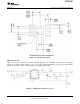
Inductor Selection
To calculate the minimum value of the output inductor, use Equation 4:
(4)
K
IND
is a coefficient that represents the amount of inductor ripple current relative to the maximum output current.
Three things need to be considered when determining the amount of ripple current in the inductor: the
peak-to-peak ripple current affects the output ripple voltage amplitude, the ripple current affects the peak switch
current, and the amount of ripple current determines at what point the circuit becomes discontinuous. For
designs using the TPS5450, K
IND
of 0.2 to 0.3 yields good results. Low output ripple voltages can be obtained
when paired with the proper output capacitor, the peak switch current will be well below the current limit set point,
and relatively low load currents can be sourced before discontinuous operation.
For this design example use K
IND
= 0.2 and the minimum inductor value is calculated to be 10.4 μH. A higher
standard value is 15 μH, which is used in this design.
Copyright © 2008–2011, Texas Instruments Incorporated Submit Documentation Feedback 13
Product Folder Link(s): TPS5450-Q1