
Datasheet


DV
IN
+
I
OUT(MAX)
0.25
C
BULK
ƒ
sw
)
ǒ
I
OUT(MAX)
ESR
MAX
Ǔ
I
CIN
+
I
OUT(MAX)
2
TPS5450-Q1
SLVS834A –JULY 2008– REVISED OCTOBER 2011
www.ti.com
Design Procedure
The following design procedure can be used to select component values for the TPS5450. Alternately, the
SWIFT™ Designer Software may be used to generate a complete design. The SWIFT™ Designer Software uses
an iterative design procedure and accesses a comprehensive database of components when generating a
design. This section presents a simplified discussion of the design process.
To begin the design process a few parameters must be decided upon. The designer needs to know the following:
• Input voltage range
• Output voltage
• Input ripple voltage
• Output ripple voltage
• Output current rating
• Operating frequency
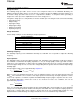
Design Parameters
For this design example, use the following as the input parameters:
DESIGN PARAMETER
(1)
EXAMPLE VALUE
Input voltage range 10 V to 31 V
Output voltage 5 V
Input ripple voltage 400 mV
Output ripple voltage 30 mV
Output current rating 5 A
Operating frequency 500 kHz
(1) As an additional constraint, the design is set up to be small size and low component height.
Switching Frequency
The switching frequency for the TPS5450 is internally set to 500 kHz. It is not possible to adjust the switching
frequency.
Input Capacitors
The TPS5450 requires an input decoupling capacitor and, depending on the application, a bulk input capacitor.
The minimum recommended decoupling capacitance is 4.7 μF. A high-quality ceramic type X5R or X7R is
required. For some applications, a smaller value decoupling capacitor may be used, so long as the input voltage
and current ripple ratings are not exceeded. The voltage rating must be greater than the maximum input voltage,
including ripple.
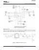
This input ripple voltage can be approximated by Equation 2 :
(2)
Where I
OUT(MAX)
is the maximum load current, f
SW
is the switching frequency, C
IN
is the input capacitor value and
ESR
MAX
is the maximum series resistance of the input capacitor. For this design, the input capacitance consists
of two 4.7 μF capacitors, C1 and C4, in parallel. An additional high-frequency bypass capacitor, C5 is also used.
The maximum RMS ripple current also needs to be checked. For worst case conditions, this can be
approximated by Equation 3 :
(3)
In this case the input ripple voltage would be 281 mV and the RMS ripple current would be 2.5 A. The maximum
voltage across the input capacitors would be VIN max plus delta VIN/2. The chosen input decoupling capacitor is
rated for 50 V, and the ripple current capacity is greater than 2.5 A each, providing ample margin. It is very
important that the maximum ratings for voltage and current are not exceeded under any circumstance.
12 Submit Documentation Feedback Copyright © 2008–2011, Texas Instruments Incorporated
Product Folder Link(s): TPS5450-Q1