
Datasheet

SLVS336B − DECEMBER 2000 − REVISED JANUARY 2007
7
detailed description (continued)
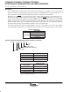
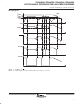
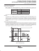
25 µs
200 ms
100 µA
t
I
BAT
Figure 1. BATTOK Timing
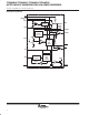
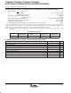
chip-enable signal gating
The internal gating of chip-enable signals (CE) prevents erroneous data from corrupting CMOS RAM during
an under-voltage condition. The TPS3600 use a series transmission gate from CEIN to CEOUT. During normal
operation (reset not asserted), the CE transmission gate is enabled and passes all CE transitions. When reset
is asserted, this path becomes disabled, preventing erroneous data from corrupting the CMOS RAM. The short
CE propagation delay from CEIN
to CEOUT enables the TPS3600 devices to be used with most processors.
The CE transmission gate is disabled and CEIN
is high impedance (disable mode) while reset is asserted.
During a power-down sequence when V
DD
crosses the reset threshold, the CE transmission gate will be
disabled and CEIN
immediately becomes high impedance if the voltage at CEIN is high. If CEIN is low during
reset is asserted, the CE transmission gate will be disabled same time when CEIN
goes high, or 15 µs after reset
asserts, whichever occurs first. This will allow the current write cycle to complete during power down. When the
CE transmission gate is enabled, the impedance of CEIN
appears as a resistor in series with the load at CEOUT.
The overall device propagation delay through the CE transmission gate depends on V
OUT
, the source
impedance of the device connected to CEIN
and the load at CEOUT. To achieve minimum propagation delay,
the capacitive load at CEOUT
should be minimized, and a low-output-impedance driver be used.
During disable mode, the transmission gate is off and an active pullup connects CEOUT
to V
OUT
. This pullup
turns off when the transmission gate is enabled.
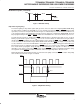
15 µs
CEIN
CEOUT
RESET
t
t
t
Figure 2. Chip-Enable Timing
www.ti.com