
Serial RapidIO (SRIO) User's Guide


www.ti.com
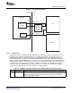
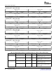
CPPIblock
CPU
DMA
Configbusaccess
L2memory
Buffer
descriptor
dual-port
SRAM
(Nx20B)
Data buffer
Peripheralboundary
32
32
32
128
CPPI control
registers
2.3.4.2 TX Operation
SRIO Functional Description
Figure 21. CPPI Boundary Diagram
Outgoing messages are handled similarly, with buffer descriptor queues that are assigned by the CPUs.
The queues are configured and initialized upon reset. When a CPU wants to send a message to an
external RapidIO device, it writes the buffer descriptor information via the configuration bus into the
SRAM. Again, there is a single buffer descriptor per RapidIO message. Upon completion of writing the
buffer descriptor, the OWNERSHIP bit is set to give control to the peripheral. The CPU then writes the TX
DMA State HDP register to initiate the queue transmit. For TX operation, PortID is specified to direct the
outgoing packet to the appropriate port. Table 19 and Table 20 describe the TX DMA state registers.
Figure 22 shows the TX buffer descriptor fields and Table 21 describes them. A TX buffer descriptor is a
contiguous block of four 32-bit data words aligned on a 32-bit boundary.
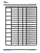
Table 19. TX DMA State Head Descriptor Pointer (HDP) (Address Offset 500h–53Ch)
Bit Name Description
31–0 TX Queue Head TX Queue Head Descriptor Pointer: This field is the DSP core memory address for the first buffer
Descriptor Pointer descriptor in the transmit queue. This field is written by the DSP core to initiate queue transmit
operations and is zeroed by the port when all packets in the queue have been transmitted. An error
condition results if the DSP core writes this field when the current field value is nonzero. The
address must be 32-bit word aligned.
SPRUE13A – September 2006 Serial RapidIO (SRIO) 51
Submit Documentation Feedback