
Datasheet


HSPCLK
PLL
X1/XCLKIN
X2
Power
Modes
Control
Watchdog
Block
C28x CPU
High-Speed Peripherals
EV-A/B
High-Speed Prescaler
Low-Speed Prescaler
Clock Enables
System
Control
Registers
Peripheral
Registers
XF_XPLLDIS
ADC
Registers
12-Bit ADC
16 ADC Inputs
HSPCLK
LSPCLK
Peripheral Reset
SYSCLKOUT
XRS
Reset
Peripheral Bus
GPIO
MUX
GPIOs
I/O
I/O
I/O
OSC
CLKIN
(A)
Low-Speed Peripherals
SCI-A/B, SPI, McBSP
Peripheral
Registers
eCAN
Peripheral
Registers
TMS320F2810, TMS320F2811, TMS320F2812
TMS320C2810, TMS320C2811, TMS320C2812
SPRS174T –APRIL 2001–REVISED MAY 2012
www.ti.com
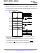
3.7 System Control
This section describes the F281x and C281x oscillator, PLL and clocking mechanisms, the watchdog
function and the low-power modes. Figure 3-8 shows the various clock and reset domains in the F281x
and C281x devices that will be discussed.
A. CLKIN is the clock input to the CPU. SYSCLKOUT is the output clock of the CPU. They are of the same frequency.
Figure 3-8. Clock and Reset Domains
48 Functional Overview Copyright © 2001–2012, Texas Instruments Incorporated
Submit Documentation Feedback
Product Folder Link(s): TMS320F2810 TMS320F2811 TMS320F2812 TMS320C2810 TMS320C2811 TMS320C2812