
Video Port/VCXO Interpolated Control (VIC) Port User's Guide


www.ti.com
Cr Buffer (1280
bytes)
Cb Buffer
(1280 bytes)
CRDST
CBDST
64
64
VDOUT[19−12]
8
8
Y Buffer
(2560 bytes)
YDSTA
64
VDOUT[9−2]
Display FIFO
8
1.3 Video Port Registers
Video Port Registers
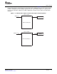
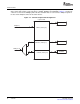
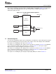
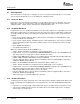
For Y/C video display, the FIFO is configured as a single channel split into separate Y, Cb, and Cr buffers
with separate read pointers and write registers (YDSTA, CBDST, and CRDST). Figure 1-10 shows how Y
data is output on the VDOUT[9-2] half of the bus and Cb/Cr data is multiplexed and output on the
VDOUT[19-12] half of the bus.
Figure 1-10. Y/C Video Display FIFO Configuration
The video port configuration register space is divided into several different sections with registers grouped
by function including top-level video port control, video capture control, video display control, and GPIO.
The registers for controlling the video port are in Section 2.4 .
The registers for controlling the video capture mode of operation are shown in Section 3.13 . An additional
space is dedicated for FIFO read pseudo-registers as shown in Section 3.14 . This space requires
high-speed access and is not mapped to the register access bus.
The registers for controlling the video display mode of operation are shown in Section 4.12 . An additional
space is dedicated for FIFO write pseudo-registers as shown in Section 4.14 . This space requires
high-speed access and is not mapped to the register access bus.
The registers for controlling the general-purpose input/output (GPIO) are shown in Section 5.1 .
SPRUEM1 – May 2007 Overview 25
Submit Documentation Feedback