
Video Port/VCXO Interpolated Control (VIC) Port User's Guide

www.ti.com
5.1.5 Video Port Pin Data Input Register (PDIN)
GPIO Registers
PDIN reflects the state of the video port pins. When read, PDIN returns the value from the pin's input
buffer (with appropriate synchronization) regardless of the state of the corresponding PFUNC or PDIR bit.
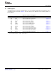
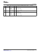
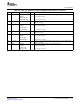
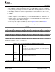
The read-only video port pin data input register (PDIN) is shown in Figure 5-5 and described in Table 5-6 .
Figure 5-5. Video Port Pin Data Input Register (PDIN)
31 24
Reserved
R-0
23 22 21 20 19 18 17 16
Reserved PDIN22 PDIN21 PDIN20 PDIN19 PDIN18 PDIN17 PDIN16
R-0 R-0 R-0 R-0 R-0 R-0 R-0 R-0
15 14 13 12 11 10 9 8
PDIN15 PDIN14 PDIN13 PDIN12 Reserved Reserved PDIN9 PDIN8
R-0 R-0 R-0 R-0 R-0 R-0 R-0 R-0
7 6 5 4 3 2 1 0
PDIN7 PDIN6 PDIN5 PDIN4 PDIN3 PDIN2 Reserved Reserved
R-0 R-0 R-0 R-0 R-0 R-0 R-0 R-0
LEGEND: R/W = Read/Write; R = Read only; - n = value after reset
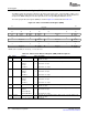
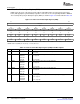
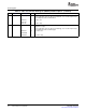
Table 5-6. Video Port Pin Data Input Register (PDIN) Field Descriptions
Bit field
(1)
symval
(1)
Value Description
31-23 Reserved - 0 Reserved. The reserved bit location is always read as 0. A value written to this field
has no effect.
22 PDIN22 OF( value) PDIN22 bit returns the logic level of the VCTL3 pin.
DEFAULT 0 Pin is logic low.
VCTL3LO
VCTL3HI 1 Pin is logic high.
21 PDIN21 OF( value) PDIN21 bit returns the logic level of the VCTL2 pin.
DEFAULT 0 Pin is logic low.
VCTL2LO
VCTL2HI 1 Pin is logic high.
20 PDIN20 OF( value) PDIN20 bit returns the logic level of the VCTL1 pin.
DEFAULT 0 Pin is logic low.
VCTL1LO
VCTL1HI 1 Pin is logic high.
19-2 PDIN[19-2] OF( value) PDIN[19-2] bit returns the logic level of the corresponding VDATA[ n] pin.
DEFAULT 0 Pin n is logic low.
VDATA nLO
VDATA nHI 1 Pin n is logic high.
(1)
For CSL implementation, use the notation VP_PDIN_PDIN n_ symval
General-Purpose I/O Operation158 SPRUEM1 – May 2007
Submit Documentation Feedback