
Video Port/VCXO Interpolated Control (VIC) Port User's Guide


www.ti.com
4.12.28 Video Display Field 2 Vertical Blanking Bit Register (VDVBIT2)
Video Display Registers
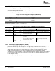
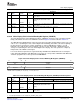
Table 4-32. Video Display Field 1 Vertical Blanking Bit Register (VDVBIT1) Field Descriptions
Description
Bit field
(1)
symval
(1)
Value BT.656 and Y/C Mode Raw Data Mode
31-28 Reserved - 0 Reserved. The reserved bit location is always read as 0. A value written to this field
has no effect.
27-16 VBITCLR1 OF( value) 0-FFFh Specifies the first line with an EAV of V = Not used.
0 indicating the start of field 1 active
display.
DEFAULT 0
15-12 Reserved - 0 Reserved. The reserved bit location is always read as 0. A value written to this field
has no effect.
11-0 VBITSET1 OF( value) 0-FFFh Specifies the first line with an EAV of V = Not used.
1 indicating the start of field 1 vertical
blanking.
DEFAULT 0
(1)
For CSL implementation, use the notation VP_VDVBIT1_ field_ symval
The video display field 2 vertical blanking bit register (VDVBIT2) controls the V bit in the EAV and SAV
timing control words for field 2. The VDVBIT2 is shown in Figure 4-59 and described in Table 4-33 .
The VBITSET2 and VBITCLR2 bits control the V bit value in the EAV and SAV timing control codes. The
V bit is set to 1 (indicating the start of field 2 digital vertical blanking) in the EAV code at the beginning of
the line whenever the frame line counter (FLCOUNT) is equal to VBITSET2. It remains a 1 for all
EAV/SAV codes until the EAV at the beginning of the line on when FLCOUNT = VBITCLR2 where it
changes to 0 (indicating the start of the field 2 digital active display). The V bit operation is completely
independent of the VBLNK control signal.
For correct interlaced operation, the region defined by VBITSET2 and VBITCLR2 must not overlap the
region defined by VBITSET1 and VBITCLR1. For progressive scan operation, VBITSET2 and VBITCLR2
should be programmed to a value greater than FRMHEIGHT.
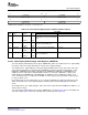
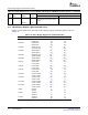
Figure 4-59. Video Display Field 2 Vertical Blanking Bit Register (VDVBIT2)
31 28 27 16
Reserved VBITCLR2
R-0 R/W-0
15 12 11 0
Reserved VBITSET2
R-0 R/W-0
LEGEND: R/W = Read/Write; R = Read only; - n = value after reset
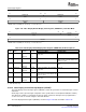
Table 4-33. Video Display Field 2 Vertical Blanking Bit Register (VDVBIT2) Field Descriptions
Description
Bit field
(1)
symval
(1)
Value BT.656 and Y/C Mode Raw Data Mode
31-28 Reserved - 0 Reserved. The reserved bit location is always read as 0. A value written to this field
has no effect.
27-16 VBITCLR2 OF( value) 0-FFFh Specifies the first line with an EAV of V = Not used.
0 indicating the start of field 2 active
display.
DEFAULT 0
15-12 Reserved - 0 Reserved. The reserved bit location is always read as 0. A value written to this field
has no effect.
(1)
For CSL implementation, use the notation VP_VDVBIT2_ field_ symval
SPRUEM1 – May 2007 Video Display Port 147
Submit Documentation Feedback