
Video Port/VCXO Interpolated Control (VIC) Port User's Guide


www.ti.com
4.12.24 Video Display Default Display Value Register (VDDEFVAL)
Video Display Registers
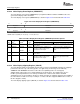
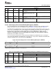
Figure 4-53. Video Display Clipping Register (VDCLIP)
31 24 23 16
CLIPCHIGH CLIPCLOW
R/W-1111-0000 R/W-0001-0000
15 8 7 0
CLIPYHIGH CLIPYLOW
R/W-1110-1011 R/W-0001-0000
LEGEND: R/W = Read/Write; R = Read only; - n = value after reset
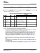
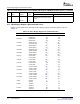
Table 4-28. Video Display Clipping Register (VDCLIP) Field Descriptions
Description
Bit field
(1)
symval
(1)
Value BT.656 and Y/C Mode Raw Data Mode
31-24 CLIPCHIGH OF( value) 0-FFh A Cb or Cr value greater than Not used.
CLIPCHIGH is forced to the CLIPCHIGH
value.
DEFAULT F0h
23-16 CLIPCLOW OF( value) 0-FFh A Cb or Cr value less than CLIPCLOW is Not used.
forced to the CLIPCLOW value.
DEFAULT 10h
15-8 CLIPYHIGH OF( value) 0-FFh A Y value greater than CLIPYHIGH is Not used.
forced to the CLIPYHIGH value.
DEFAULT EBh
7-0 CLIPYLOW OF( value) 0-FFh A Y value less than CLIPYLOW is forced Not used.
to the CLIPYLOW value.
DEFAULT 10h
(1)
For CSL implementation, use the notation VP_VDCLIP_ field_ symval
The video display default display value register (VDDEFVAL) defines the default value to be output during
the portion of the active video window that is not part of the displayed image.
The default value is output during the non-image display window portions of the active video. This is the
region between ILCOUNT = 0 and ILCOUNT = IMGVOFF n vertically, and between IPCOUNT = 0 and
IPCOUNT = IMGHOFF n horizontally. In BT.656 mode, CBDEFVAL, YDEFVAL, and CRDEFVAL are
multiplexed on the output in the standard CbYCrY manner. In Y/C mode, YDEFVAL is output on the
VDOUT[9-2] bus and CBDEFVAL and CRDEFVAL are multiplexed on the VDOUT[19-12] bus. In all
cases, the default values are output on the 8 MSBs of the bus ([9-2] or [19-12]) and the 2 LSBs ([1-0] or
[11-10]) are driven as 0s.
In raw data mode, the least significant 8, 10, 16, or 20 bits of DEFVAL are output depending on the bus
width. The default value is also output during the horizontal and vertical blanking periods in raw data
mode.
The default value is also output during the entire active video region when the BLKDIS bit in VDCTL is set
and the FIFO is empty.
The video display default display value register (VDDEFVAL) is shown in Figure 4-54 for the BT.656 and
Y/C modes and in Figure 4-55 for the raw data mode, and described in Table 4-29 .
SPRUEM1 – May 2007 Video Display Port 143
Submit Documentation Feedback