
Video Port/VCXO Interpolated Control (VIC) Port User's Guide

www.ti.com
4.2.2 Blanking Codes
4.2.3 BT.656 Image Display
4.2.4 BT.656 FIFO Unpacking
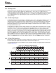
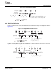
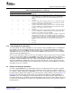
VDOUT[9−2]
VCLKOUT
63 5655 4847 4039 32
Y FIFO
Cb FIFO
Cb 0 Cr 0 Cb 1 Cr 1Y 0 Y 1 Y 2 Y 3 Cb 2 Cr 2Y 4 Y 5
Cr FIFO
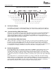
Little-Endian Unpacking
31 2423 1615 8 7 0
Y 25
Y 17
Y 9
Y 1
Y 24
Y 16
Y 8
Y 0
Y 27
Y 19
Y 11
Y 3
Y 26
Y 18
Y 10
Y 2
Y 29
Y 21
Y 13
Y 5
Y 28
Y 20
Y 12
Y 4
Y 31
Y 23
Y 15
Y 7
Y 30
Y 22
Y 14
Y 6
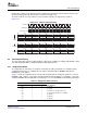
63 5655 4847 4039 3231 2423 1615 8 7 0
Cb 9
Cb 1
Cb 8
Cb 0
Cb 11
Cb 3
Cb 10
Cb 2
Cb 13
Cb 5
Cb 12
Cb 4
Cb 15
Cb 7
Cb 14
Cb 6
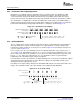
63 5655 4847 4039 3231 2423 1615 8 7 0
Cr 9
Cr 1
Cr 8
Cr 0
Cr 11
Cr 3
Cr 10
Cr 2
Cr 13
Cr 5
Cr 12
Cr 4
Cr 15
Cr 7
Cr 14
Cr 6
BT.656 Video Display Mode
The time between the EAV and SAV code on each line represents the horizontal blanking interval. During
this time, the video port outputs digital video blanking values. These values are 10.0h for luma (Y)
samples and 80.0h for chroma (Cb/Cr) samples. These values are also output during the active line period
of vertical blanking (between SAV and EAV when V = 1). In addition, if the DVEN bit in VDCTL is cleared
to 0, the blanking values are output during the portion of active video lines that are not a part of the
displayed image.
For BT.656 display mode, the FIFO buffer is divided into three sections. One FIFO is 2560-bytes deep and
is used for the storage of Y output samples; the other two FIFOs are each 1280-bytes deep and are
dedicated for storage of Cb and Cr samples. Each FIFO has a memory-mapped location associated with
it; YDST, CBDST, and CRDST. The pseudo-registers are write-only and are used by EDMAs to fill the
FIFOs with output data. The video display module multiplexes the data from the three FIFOs to generate
the output CbYCrY data stream.
If video display is enabled, the video display module uses the YEVT, CbEVT, and CrEVT events to notify
the EDMA controller that data needs to be placed into the display FIFOs. The number of pixels required to
generate the events is set by the threshold field bits in VDTHRLD register. The video display module
generates the event signals when the display buffer holds less than the threshold number of pixels and the
display event counter has not expired. On every YEVT, the EDMA should move data from DSP memory to
the Y buffer, using the Y FIFO destination register (YDST) content as the destination address. On every
CbEVT, the EDMA should move data from DSP memory to the Cb buffer, using the Cb FIFO destination
register (CBDST) content as the destination address. On every CrEVT, the EDMA should move data from
DSP memory to the Cr buffer, using the Cr FIFO destination register (CRDST) content as the destination
address. The EDMA transfer size for the Y buffer is twice the size of the EDMA for the Cb or Cr buffers.
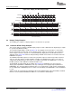
Display data is always packed into the FIFOs in 64-bit words and must be unpacked before being sent to
the video display data pipeline. By default, data is unpacked from right to left.
The 8-bit BT.656 mode uses three FIFOs for color separation. Samples are unpacked from each word as
shown in Figure 4-12 .
Figure 4-12. 8-Bit BT.656 FIFO Unpacking
SPRUEM1 – May 2007 Video Display Port 101
Submit Documentation Feedback