
DSP Subsystem Reference Guide

www.ti.com
5.4.3 PLL Control Register (PLLCTL)
PLL Controller Registers
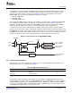
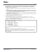
The PLL control register (PLLCTL) is shown in Figure 5-5 and described in Table 5-7 .
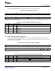
Figure 5-5. PLL Control Register (PLLCTL)
31 16
Reserved
R-0
15 9 8 7 6 5 4 3 2 1 0
Reserved CLKMODE Reserved PLLENSRC PLLDIS PLLRST Rsvd PLLPWRDN PLLEN
R-0 R/W-0 R-1h R/W-1 R/W-1 R/W-0 R-0 R/W-1 R/W-0
LEGEND: R/W = Read/Write; R = Read only; - n = value after reset
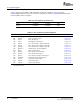
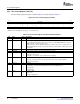
Table 5-7. PLL Control Register (PLLCTL) Field Descriptions
Bit Field Value Description
31-9 Reserved 0 Reserved
8 CLKMODE Reference clock selection
0 Internal oscillator. If the device reference clock source is a crystal at MXI/CLKIN pin, the internal
oscillator must be selected as the clock source.
1 CLKIN square wave. This mode applies if the device reference clock source is a square wave at
MXI/CLKIN pin. When this mode is selected, the PLLC turns off the internal oscillator's bias resistor
to save power.
7-6 Reserved 1 Reserved
5 PLLENSRC 0 This bit must be cleared to 0 before PLLEN will have any effect.
4 PLLDIS Asserts DISABLE to PLL.
0 PLL disable is de-asserted.
1 PLL disable is asserted. PLL output is disabled and not toggling.
3 PLLRST Asserts RESET to PLL if supported.
0 PLL reset is asserted. See device-specific data manual for the PLL reset time required.
1 PLL reset is not asserted.
2 Reserved 0 Reserved
1 PLLPWRDN PLL power-down. After powering up the PLL (PLLPWRDN 1 to 0 transition), you must wait for the
PLL to stabilize. See device-specific data manual for the PLL stabilization time.
0 PLL operational.
1 PLL power-down.
0 PLLEN PLL mode enable.
0 Bypass mode
1 PLL mode, not bypassed
50 PLL Controller SPRU978E – March 2008
Submit Documentation Feedback