
DSP Subsystem Reference Guide

www.ti.com
5.3 PLL2 Control
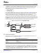
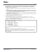
PLLDIV2 (/10)
PLLDIV1 (/2)
1
0
PLLM
PLL
0
1
BPDIV
CLKMODE
CLKIN
OSCIN
PLLEN
PLL2_SYSCLK2
(VPSS−VPBE)
PLL2_SYSCLK1
(DDR2 PHY)
PLL2_SYSCLKBP
(DDR2 VTP)
PLLOUT
5.3.1 Device Clock Generation
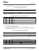
PLL2 Control
PLL2 provides the clock from which the DDR2 memory controller and optional VPBE clocks are derived.
The DDR PLL controller 2 (PLLC2) controls PLL2, which accepts the clock from the oscillator and also
generates the various frequency clocks needed. Figure 5-2 shows the customization of PLL2 in the
DM643x DMP. The PLL2 clocks are distributed to the device as follows:
• SYSCLK1: DDR2 PHY
• SYSCLK2: VPSS
• SYSCLKBP: DDR2 VTP
PLL2 supplies the DDR2 memory controller clock. Software controls the PLL2 operation through the DDR
PLL controller 2 (PLLC2) registers. The registers used in PLLC2 are listed in Section 5.4 . The PLL2
multiplier is controlled by the PLLM bit of the PLL multiplier control register (PLLM). The PLL2 multiplier
may be modified by software (for example, to tune the DDR interface for best performance).
The PLL2 output clock must be divided-down to the DDR operating range using the SYSCLK1 divider.
At power-up, PLL2 is powered-down and disabled, and must be powered-up by software through the PLL2
PLLPWRDN bit in the PLL control register (PLLCTL). By default, the system operates in bypass mode and
the DDR clock is provided directly from the input reference clock. Once the PLL is powered-up and locked,
software can switch the device to PLL mode operation by setting the PLLEN bit in PLLCTL to 1.
Figure 5-2. PLL2 Structure in the TMS320DM643x DMP
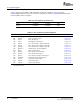
PLLC2 generates two clocks from the PLL2 output clock for use by the DDR2 memory controller and
VPSS modules. These are summarized in Table 5-2 .
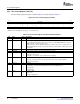
Table 5-2. DDR PLLC2 Output Clocks
Output Clock Used by Default Divider
SYSCLK2 VPSS /10
SYSCLK1 DDR Phy /2
SYSCLKBP DDR VTP Controller /2
The SYSCLK1 output clock divider value defaults to /2. Assuming a 27 MHZ MXI/CLKIN and the PLL2
default multiplier of × 20, this results in a 270 MHZ DDR Phy clock (135 MHZ DDR2). It can be modified by
software (RATIO bit in PLLDIV1) in combination with other PLL multipliers to achieve the desired DDR
clock rate. The SYSCLK2 divider is programmable to allow a 54 MHZ output to be generated from any
even-multiple PLL output frequency for use by the VPSS.
SPRU978E – March 2008 PLL Controller 43
Submit Documentation Feedback