
DSP Subsystem Reference Guide

www.ti.com
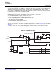
PLLDIV1(/1)
PLLDIV3(/6)
PLLDIV2(/3)
SYSCLK1
(CLKDIV1Domain)
SYSCLK3
(CLKDIV6Domain)
SYSCLK2
(CLKDIV3Domain)
1
0
PLLM
PLL
0
1
BPDIV
CLKMODE
CLKIN
OSCIN
PLLEN
SYSCLKBP
(VPSS-VPBR
ClockSource)
OBSCLK
(CLKOUT0Pin)
PLLOUT
AUXCLK
(CLKINDomain)
OSCDIV1
5.2.1 Device Clock Generation
5.2.2 Steps for Changing PLL1/Core Domain Frequency
PLL1 Control
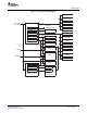
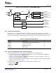
Figure 5-1. PLL1 Structure in the TMS320DM643x DMP
PLLC1 generates several clocks from the PLL1 output clock for use by the various processors and
modules. These are summarized in Table 5-1 . SYSCLK1, SYSCLK2, and SYSCLK3 must maintain a fixed
frequency ratio requirement, no matter what reference clock (PLL or bypass) or PLL frequency is used.
Table 5-1. System PLLC1 Output Clocks
PLLC1 Output Clock Used by Default Divider
SYSCLK1 DSP Subsystem /1
SYSCLK2 SCR, EDMA, VPSS, CLKDIV3 Domain peripherals /3
SYSCLK3 CLKDIV6 Domain peripherals /6
AUXCLK CLKIN Domain peripherals NA
OBSCLK CLKOUT0 source /1
SYSCLKBP VPBE clock source /1
Refer to the appropriate subsection on how to program the PLL1/Core Domain clocks:
• If the PLL is powered down (PLLPWRDN bit in PLLCTL is set to 1), follow the full PLL initialization
procedure in Section 5.2.2.1 to initialize the PLL.
• If the PLL is not powered down (PLLPWRDN bit in PLLCTL is cleared to 0), follow the sequence in
Section 5.2.2.2 to change the PLL multiplier.
• If the PLL is already running at a desired multiplier and you only want to change the SYSCLK dividers,
follow the sequence in Section 5.2.2.3 .
Note that the PLL is powered down after the following device-level global resets:
• Power-on Reset ( POR)
• Warm Reset ( RESET)
• Max Reset
SPRU978E – March 2008 PLL Controller 39
Submit Documentation Feedback