
DSP Subsystem Reference Guide

www.ti.com
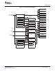
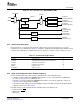
4.2.4 I/O Domains
Clock Domains
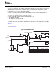
The I/O domains refer to the frequencies of the peripherals that communicate through device pins. In
many cases, there are frequency requirements for a peripheral pin interface that are set by an outside
standard and must be met. It is not necessarily possible to obtain these frequencies from the on-chip clock
generation circuitry, so the frequencies must be obtained from external sources and are asynchronous to
the core frequency domain by definition.
Table 4-5 lists peripherals with external I/O interface, and their I/O domain clock/frequency. It also shows
the core clock domain as a reference to show the core clock used for internal communications. See
section Section 4.2.1 for more details on core clock domains. See device-specific data manual for the
exact I/O clock frequency supported on the device.
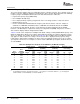
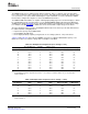
Table 4-5. Peripheral I/O Domain Clock
I/O (External) Domain Clock Source Options
I/O Domain Clock
Peripheral Frequency Internal Clock Source External Clock Source Core Clock Domain
DDR2 125-166 MHZ PLLC2 SYSCLK1 — CLKDIV3
VPFE 10-98 MHZ — PCLK CLKDIV3
VPBE 6.25-75 MHZ PLLC1 SYSCLKBP VPBECLK CLKDIV3
(typically 27 MHZ)
PLLC2 SYSCLK2 PCLK
(typically 54 MHZ)
PCI 33 MHZ — PCICLK CLKDIV3
EMAC 25 MHZ — MTXCLK, MRXCLK CLKDIV6
VLYNQ up to 80 MHZ PLLC1 SYSCLK3 VLYNQ_CLOCK CLKDIV6
McBSP up to 40 MHZ PLLC1 SYSCLK3 CLKS, CLKX, CLKR CLKDIV6
McASP up to 40 MHZ PLLC1 SYSCLK3 AHCLKX, AHCLKR, CLKDIV6
ACLKX, ACLKR
GPIO NA (asynchronous — — CLKDIV6
interface)
EMIFA NA (asynchronous — — CLKDIV6
interface)
HPI NA (asynchronous — — CLKDIV6
interface)
I2C up to 400 kHz MXI/CLKIN SCL CLKIN
(typically 27 MHZ)
Timer output up to 1/2 CLKIN MXI/CLKIN TINP0L (Timer 0), CLKIN
frequency (typically 27 MHZ) TINP1L (Timer 1)
input up to 1/4 CLKIN
frequency
Watchdog Timer NA MXI/CLKIN — CLKIN
(typically 27 MHZ)
PWM NA — — CLKIN
UART NA — — CLKIN
HECC NA — — CLKIN
34 Device Clocking SPRU978E – March 2008
Submit Documentation Feedback