
DSP Subsystem Reference Guide


www.ti.com
1.1 Introduction
1.2 Block Diagram
JTAG Interface
System Control
PLLs/Clock Generator
Input
Clock(s)
Power/Sleep Controller
Pin Multiplexing
DSP Subsystem
C64x+t DSP CPU
32 KB
L1 Pgm
128 KB L2 RAM
80 KB
L1 Data
BT.656,
Y/C,
Raw (Bayer)
Video Processing Subsystem (VPSS)
CCD
Controller
Video
Interface
Front End
Resizer
Histogram/
3A
Preview
10b DAC
On-Screen
Display
(OSD)
Video
Encoder
(VENC)
10b DAC
10b DAC
10b DAC
Back End 8b BT.656,
Y/C,
24b RGB
NTSC/
PAL,
S-Video,
RGB,
YPbPr
Switched Central Resource (SCR)
Peripherals
EDMA
I
2
C HECC UART
Serial Interfaces
DDR2
Mem Ctlr
(32b)
Async EMIF/
NAND/
(8b)
Program/Data Storage
Watchdog
Timer
PWM
System
General-
Purpose
Timer
PCI
(33 MHz)
VLYNQ
EMAC
With
MDIO
Connectivity
HPI
McASP McBSP
OSC
Boot ROM
16b
GPIO
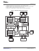
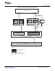
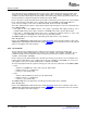
Introduction
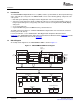
The TMS320DM643x Digital Media Processor (DMP) contains a powerful DSP to efficiently handle image,
video, and audio processing tasks. The DM643x DMP consists of the following primary components and
sub-systems:
• DSP Subsystem (DSPSS), including the C64x+ Megamodule and associated memory.
• Video Processing Subsystem (VPSS), including the Video Processing Front End (VPFE) Subsystem,
Image Input and Image Processing Subsystem, and the Video Processing Back End (VPBE) Display
Subsystem
• A set of I/O peripherals
• A powerful DMA subsystem and DDR2 memory controller interface
The DSP subsystem includes TI’s standard TMS320C64x+ Megamodule and several blocks of internal
memory (L1P, L1D, and L2).
For more information, see the TMS320C64x+ DSP Megamodule Peripherals Reference Guide
(SPRU871 ), the TMS320C64x/C64x+ DSP CPU and Instruction Set Reference Guide (SPRU732 ), and the
TMS320C64x+ DSP Cache User’s Guide (SPRU862 ).
An example block diagram for the TMS320DM643x DMP is shown in Figure 1-1 .
Figure 1-1. TMS320DM643x DMP Block Diagram
Introduction 12 SPRU978E – March 2008
Submit Documentation Feedback