TMS320DM643x DMP Universal Asynchronous Receiver/Transmitter (UART) User's Guide Literature Number: SPRU997C December 2009
SPRU997C – December 2009 Submit Documentation Feedback Copyright © 2009, Texas Instruments Incorporated
Preface ....................................................................................................................................... 6 1 Introduction ........................................................................................................................ 7 .............................................................................................. 7 .................................................................................................................. 7 1.
www.ti.com List of Figures 1 UART Block Diagram ....................................................................................................... 9 2 UART Clock Generation Diagram ....................................................................................... 10 3 Relationships Between Data Bit, BCLK, and UART Input Clock .................................................... 11 4 UART Protocol Formats ......................................................................................
www.ti.com List of Tables 1 UART Supported Features/Characteristics by Instance ............................................................... 8 2 Baud Rate Examples for 27 MHz UART Input Clock ................................................................. 11 3 UART Signal Descriptions ................................................................................................ 12 4 Character Time for Word Lengths ...............................................................................
Preface SPRU997C – December 2009 Read This First About This Manual This document describes the universal asynchronous receiver/transmitter (UART) peripheral in the TMS320DM643x Digital Media Processor (DMP) . Notational Conventions This document uses the following conventions. • Hexadecimal numbers are shown with the suffix h. For example, the following number is 40 hexadecimal (decimal 64): 40h. • Registers in this document are shown in figures and described in tables.
User's Guide SPRU997C – December 2009 Universal Asynchronous Receiver/Transmitter (UART) 1 Introduction This document describes the universal asynchronous receiver/transmitter (UART) peripheral in the TMS320DM643x Digital Media Processor (DMP) . 1.1 Purpose of the Peripheral The UART peripheral is based on the industry standard TL16C550 asynchronous communications element, which in turn is a functional upgrade of the TL16C450.
Introduction www.ti.com Table 1 summarizes the capabilities supported on the UART. Note that the number of UARTs and their supported features vary on each device, see the device-specific data manual for more details. Table 1. UART Supported Features/Characteristics by Instance Feature Support 5, 6, 7 or 8-bit characters Supported Even, odd, or no PARITY bit Supported 1, 1.
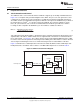
Introduction www.ti.com Figure 1.
Peripheral Architecture www.ti.com 2 Peripheral Architecture 2.1 Clock Generation and Control The UART bit clock is sourced from the PLLC1 AUXCLK. It supports up to 128 kbps maximum data rate. Figure 2 is a conceptual clock generation diagram for the UART. The processor clock generator receives a signal from an external clock source and produces a UART input clock with a programmed frequency.
Peripheral Architecture www.ti.com Figure 3. Relationships Between Data Bit, BCLK, and UART Input Clock n UART input clock cycles, where n = divisor in DLH:DLL UART input clock n BCLK Each bit lasts 16 BCLK cycles. When receiving, the UART samples the bit in the 8th cycle. BCLK TX, RX D1 D2 D0 TX, RX START D0 D1 D2 D3 D4 D5 D6 D7 PARITY STOP1 STOP2 Table 2. Baud Rate Examples for 27 MHz UART Input Clock Baud Rate Divisor Value Actual Baud Rate Error (%) 2400 703 2400.427 0.
Peripheral Architecture 2.2 www.ti.com Signal Descriptions The UARTs utilize a minimal number of signal connections to interface with external devices. The UART signal descriptions are included in Table 3. Note that the number of UARTs and their supported features vary on each device, see the device-specific data manual for more details. Table 3.
Peripheral Architecture www.ti.com 2.4.3 Data Format The UART transmits in the following format: 1 START bit + data bits (5, 6, 7, 8) + 1 PARITY bit (optional) + STOP bit (1, 1.5, 2) It transmits 1 START bit; 5, 6, 7, or 8 data bits, depending on the data width selection; 1 PARITY bit, if parity is selected; and 1, 1.5, or 2 STOP bits, depending on the STOP bit selection.
Peripheral Architecture 2.6 2.6.1 www.ti.com Operation Transmission The UART transmitter section includes a transmitter hold register (THR) and a transmitter shift register (TSR). When the UART is in the FIFO mode, THR is a 16-byte FIFO. Transmitter section control is a function of the UART line control register (LCR). Based on the settings chosen in LCR, the UART transmitter sends the following to the receiving device: • 1 START bit • 5, 6, 7, or 8 data bits • 1 PARITY bit (optional) • 1, 1.
Peripheral Architecture www.ti.com 2.6.3 FIFO Modes The following two modes can be used for servicing the receiver and transmitter FIFOs: • FIFO interrupt mode. The FIFO is enabled and the associated interrupts are enabled. Interrupts are sent to the CPU to indicate when specific events occur. • FIFO poll mode. The FIFO is enabled but the associated interrupts are disabled. The CPU polls status bits to detect specific events.
Peripheral Architecture 2.6.3.2 www.ti.com FIFO Poll Mode When the receiver FIFO is enabled in the FIFO control register (FCR) and the receiver interrupts are disabled in the interrupt enable register (IER), the poll mode is selected for the receiver FIFO. Similarly, when the transmitter FIFO is enabled and the transmitter interrupts are disabled, the transmitted FIFO is in the poll mode.
Peripheral Architecture www.ti.com 2.6.4.1 RTS Behavior RTS data flow control originates in the receiver block (see Figure 1). When the receiver FIFO level reaches a trigger level of 1, 4, 8, or 14 (see Figure 6), RTS is deasserted. The sending UART may send an additional byte after the trigger level is reached (assuming the sending UART has another byte to send), because it may not recognize the deassertion of RTS until after it has begun sending the additional byte.
Peripheral Architecture 2.7 2.7.1 www.ti.com Reset Considerations Software Reset Considerations Two bits in the power and emulation management register (PWREMU_MGMT) control resetting the parts of the UART: • The UTRST bit controls resetting the transmitter only. If UTRST = 1, the transmitter is active; if UTRST = 0, the transmitter is in reset. • The URRST bit controls resetting the receiver only. If URRST = 1, the receiver is active; if URRST = 0, the receiver is in reset.
Peripheral Architecture www.ti.com Table 5. UART Interrupt Requests Descriptions UART Interrupt Request Interrupt Source Comment THREINT THR-empty condition: The transmitter holding register (THR) or the transmitter FIFO is empty. All of the data has been copied from THR to the transmitter shift register (TSR). If THREINT is enabled in IER, by setting the ETBEI bit, it is recorded in IIR. As an alternative to using THREINT, the CPU can poll the THRE bit in the line status register (LSR).
Peripheral Architecture www.ti.com 2.10 DMA Event Support In the FIFO mode, the UART generates the following two DMA events: • Receive event (URXEVT): The trigger level for the receiver FIFO (1, 4, 8, or 14 characters) is set with the RXFIFTL bit in the FIFO control register (FCR). Every time the trigger level is reached or a receiver time-out occurs, the UART sends a receive event to the EDMA controller.
Registers www.ti.com 2.13 Exception Processing 2.13.1 Divisor Latch Not Programmed Since the processor reset signal has no effect on the divisor latch, the divisor latch will have an unknown value after power up. If the divisor latch is not programmed after power up, the baud clock (BCLK) will not operate and will instead be set to a constant logic 1 state. The divisor latch values should always be reinitialized following a processor reset. 2.13.
Registers 3.1 www.ti.com Receiver Buffer Register (RBR) The receiver buffer register (RBR) is shown in Figure 9 and described in Table 7. The UART receiver section consists of a receiver shift register (RSR) and a receiver buffer register (RBR). When the UART is in the FIFO mode, RBR is a 16-byte FIFO. Timing is supplied by the 16x receiver clock. Receiver section control is a function of the line control register (LCR). RSR receives serial data from the RX pin.
Registers www.ti.com 3.2 Transmitter Holding Register (THR) The transmitter holding register (THR) is shown in Figure 10 and described in Table 8. The UART transmitter section consists of a transmitter hold register (THR) and a transmitter shift register (TSR). When the UART is in the FIFO mode, THR is a 16-byte FIFO. Transmitter section control is a function of the line control register (LCR). THR receives data from the internal data bus and when TSR is idle, the UART moves the data from THR to TSR.
Registers 3.3 www.ti.com Interrupt Enable Register (IER) The interrupt enable register (IER) is used to individually enable or disable each type of interrupt request that can be generated by the UART. Each interrupt request that is enabled in IER is forwarded to the CPU. IER is shown in Figure 11 and described in Table 9. Access considerations: IER and DLH share one address. To read or modify IER, write 0 to the DLAB bit in LCR. When DLAB = 1, all accesses at the shared address read or modify DLH.
Registers www.ti.com 3.4 Interrupt Identification Register (IIR) The interrupt identification register (IIR) is a read-only register at the same address as the FIFO control register (FCR), which is a write-only register. When an interrupt is generated and enabled in the interrupt enable register (IER), IIR indicates that an interrupt is pending in the IPEND bit and encodes the type of interrupt in the INTID bits. IIR is shown in Figure 12 and described in Figure 12.
Registers www.ti.com Table 11. Interrupt Identification and Interrupt Clearing Information IIR Bits Priority Level 3 2 1 0 Interrupt Type Interrupt Source Event That Clears Interrupt None 0 0 0 1 None None None 1 0 1 1 0 Receiver line status Overrun error, parity error, framing error, or break is detected. For an overrun error, reading the line status register (LSR) clears the interrupt.
Registers www.ti.com Figure 13. FIFO Control Register (FCR) 31 16 Reserved R-0 15 8 Reserved R-0 7 3 2 1 0 RXFIFTL 6 5 Reserved 4 DMAMODE1 (1) TXCLR RXCLR FIFOEN W-0 R-0 W-0 W1C-0 W1C-0 W-0 LEGEND: R = Read only; W = Write only; W1C = Write 1 to clear (writing 0 has no effect); -n = value after reset (1) Always write 1 to the DMAMODE1 bit. After a hardware reset, change the DMAMODE1 bit from 0 to 1.
Registers 3.6 www.ti.com Line Control Register (LCR) The line control register (LCR) is shown in Figure 14 and described in Table 13. The system programmer controls the format of the asynchronous data communication exchange by using LCR. In addition, the programmer can retrieve, inspect, and modify the content of LCR; this eliminates the need for separate storage of the line characteristics in system memory. Figure 14.
Registers www.ti.com Table 13. Line Control Register (LCR) Field Descriptions (continued) Bit Field 2 STB Value Description Number of STOP bits generated. STB specifies 1, 1.5, or 2 STOP bits in each transmitted character. When STB = 1, the WLS bit determines the number of STOP bits. The receiver clocks only the first STOP bit, regardless of the number of STOP bits selected. The number of STOP bits generated is summarized in Table 15. 0 1 STOP bit is generated.
Registers 3.7 www.ti.com Modem Control Register (MCR) The modem control register (MCR) is shown in Figure 15 and described in Table 16. The modem control register provides the ability to enable/disable the autoflow functions, and enable/disable the loopback function for diagnostic purposes. Figure 15.
Registers www.ti.com 3.8 Line Status Register (LSR) The line status register (LSR) is shown in Figure 16 and described in Table 17. LSR provides information to the CPU concerning the status of data transfers. LSR is intended for read operations only; do not write to this register. Bits 1 through 4 record the error conditions that produce a receiver line status interrupt. Figure 16.
Registers www.ti.com Table 17. Line Status Register (LSR) Field Descriptions (continued) Bit 4 Field Value BI Description Break indicator. The BI bit is set whenever the receive data input (RX) was held low for longer than a full-word transmission time. A full-word transmission time is defined as the total time to transmit the START, data, PARITY, and STOP bits. If the BI bit is set and the corresponding interrupt enable bit is set (ELSI = 1 in IER), an interrupt request is generated.
Registers www.ti.com Table 17. Line Status Register (LSR) Field Descriptions (continued) Bit Field 0 Value DR Description Data-ready (DR) indicator for the receiver. If the DR bit is set and the corresponding interrupt enable bit is set (ERBI = 1 in IER), an interrupt request is generated. In non-FIFO mode: 0 Data is not ready, or the DR bit was cleared because the character was read from the receiver buffer register (RBR). 1 Data is ready.
Registers www.ti.com Figure 17. Divisor LSB Latch (DLL) 31 16 Reserved R-0 15 8 7 0 Reserved DLL R-0 R/W-0 LEGEND: R/W = Read/Write; R = Read only; -n = value after reset Table 18. Divisor LSB Latch (DLL) Field Descriptions Bit Field 31-8 Reserved 7-0 DLL Value 0 Description Reserved 0-Fh The 8 least-significant bits (LSBs) of the 16-bit divisor for generation of the baud clock in the baud rate generator. Maximum baud rate is 128 kbps. Figure 18.
Registers www.ti.com 3.10 Peripheral Identification Registers (PID1 and PID2) The peripheral identification registers (PID) contain identification data (class, revision, and type) for the peripheral. PID1 is shown in Figure 19 and described in Table 20. PID2 is shown in Figure 20 and described in Table 21. Figure 19. Peripheral Identification Register 1 (PID1) 31 16 Reserved R-0 15 8 7 0 CLS REV R-1h R-1h LEGEND: R = Read only; -n = value after reset Table 20.
Registers www.ti.com 3.11 Power and Emulation Management Register (PWREMU_MGMT) The power and emulation management register (PWREMU_MGMT) is shown in Figure 21 and described in Table 22. Figure 21. Power and Emulation Management Register (PWREMU_MGMT) 31 16 Reserved R-0 15 14 13 Rsvd UTRST URRST 12 Reserved 1 FREE 0 R/W-0 R/W-0 R/W-0 R-0 R/W-0 LEGEND: R/W = Read/Write; R = Read only; -n = value after reset Table 22.
www.ti.com Appendix A Revision History Table 23 lists the changes made since the previous version of this document. Table 23. Document Revision History Reference Additions/Modifications/Deletions Section 2.1 Changed first paragraph.
IMPORTANT NOTICE Texas Instruments Incorporated and its subsidiaries (TI) reserve the right to make corrections, modifications, enhancements, improvements, and other changes to its products and services at any time and to discontinue any product or service without notice. Customers should obtain the latest relevant information before placing orders and should verify that such information is current and complete.