
DDR2 Memory Controller User's Guide

www.ti.com
4.1 SDRAM Status Register (SDRSTAT)
DDR2 Memory Controller Registers
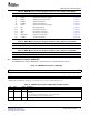
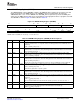
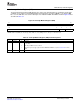
Table 22. DDR2 Memory Controller Registers Relative to Base Address 2000 0000h
Offset Acronym Register Description Section
4h SDRSTAT SDRAM Status Register Section 4.1
8h SDBCR SDRAM Bank Configuration Register Section 4.2
Ch SDRCR SDRAM Refresh Control Register Section 4.3
10h SDTIMR SDRAM Timing Register Section 4.4
14h SDTIMR2 SDRAM Timing Register 2 Section 4.5
20h PBBPR Peripheral Bus Burst Priority Register Section 4.6
C0h IRR Interrupt Raw Register Section 4.7
C4h IMR Interrupt Masked Register Section 4.8
C8h IMSR Interrupt Mask Set Register Section 4.9
CCh IMCR Interrupt Mask Clear Register Section 4.10
E4h DDRPHYCR DDR PHY Control Register Section 4.11
F0h VTPIOCR VTP IO Control Register Section 4.12
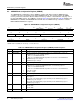
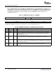
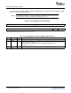
Table 23. DDR2 Memory Controller Registers Relative to Base Address 01C4 2000h
Offset Acronym Register Description Section
38h DDRVTPR DDR VTP Register Section 4.13
Table 24. DDR2 Memory Controller Registers Relative to Base Address 01C4 0000h
Offset Acronym Register Description Section
4Ch DDRVTPER DDR VTP Enable Register Section 4.14
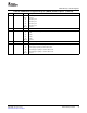
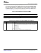
The SDRAM status register (SDRSTAT) is shown in Figure 19 and described in Table 25 .
Figure 19. SDRAM Status Register (SDRSTAT)
31 16
Reserved
R-4000h
15 3 2 1 0
Reserved PHYRDY Reserved
R-0 R-0 R-0
LEGEND: R/W = Read/Write; R = Read only; - n = value after reset; -x = value is indeterminate after reset
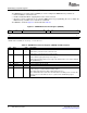
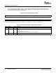
Table 25. SDRAM Status Register (SDRSTAT) Field Descriptions
Bit Field Value Description
31-3 Reserved 0 Reserved
2 PHYRDY DDR2 memory controller DLL ready. Reflects whether the DDR2 memory controller DLL is powered up
and locked.
0 DLL is not ready, either powered down, in reset, or not locked.
1 DLL is powered up, locked, and ready for operation.
1-0 Reserved 0 Reserved
SPRU986B – November 2007 DDR2 Memory Controller 41
Submit Documentation Feedback