
DDR2 Memory Controller User's Guide

www.ti.com
2.3 Signal Descriptions
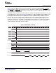
DDR_D[31:0]
DDR2
memory
controller
DDR_CLK
DDR_CLK
DDR_CS
DDR_CKE
DDR_RAS
DDR_WE
DDR_DQM[3:0]
DDR_CAS
DDR_BA[2:0]
DDR_DQS[3:0]
DDR_A[12:0]
DDR_ZN
DDR_ZP
200 Ω
200 Ω
Peripheral Architecture
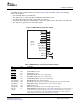
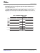
The DDR2 memory controller signals are shown in Figure 3 and described in Table 2 . The following
features are included:
• The maximum data bus is 32-bits wide.
• The address bus is 13-bits wide with an additional 3 bank address pins.
• Two differential output clocks driven by internal clock sources.
• Command signals: Row and column address strobe, write enable strobe, data strobe, and data mask.
• One chip select signal and one clock enable signal.
Figure 3. DDR2 Memory Controller Signals
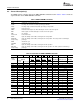
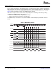
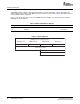
Table 2. DDR2 Memory Controller Signal Descriptions
Pin Type Description
DDR_CLK, O/Z Clock: Differential clock outputs.
DDR_CLK
DDR_CKE O/Z Clock enable: Active high.
DDR_CS O/Z Chip select: Active low.
DDR_WE O/Z Write enable strobe: Active low, command output.
DDR_RAS O/Z Row address strobe: Active low, command output.
DDR_CAS O/Z Column address strobe: Active low, command output.
DDR_DQM[3:0] O/Z Data mask: Output mask signal for write data.
DDR_DQS[3:0] I/O/Z Data strobe: Active high, bi-directional signals. Output with write data, input with read data.
DDR_BA[2:0] O/Z Bank address: Output, defining which bank a given command is applied.
DDR_A[12:0] O/Z Address: Address bus.
DDR_D[31:0] I/O/Z Data: Bi-directional data bus. Input for read data, output for write data.
DDR_ZN, O Output impedance control: Required to set the DDR2 output impedance. Connected by way of
DDR_ZP a 200-ohm resistor to power and ground (see Figure 3 ). The resistor should be chosen to be
4 times the desired impedance of the output buffer. By changing the size of the resistor, the
DDR2 outputs can be tuned to match the board load, if necessary.
SPRU986B – November 2007 DDR2 Memory Controller 11
Submit Documentation Feedback