
Universal Serial Bus Controller User's Guide

2 Peripheral Architecture
2.1 Clock Control
2.2 Signal Descriptions
2.3 Indexed and Non-Indexed Registers
www.ti.com
Peripheral Architecture
Information related to clock generation and control for the USB peripheral will be added in a future revision
of this document. Clocks for USB are generated based on a crystal oscillator on the M24XI and M24XO
pins. The oscillator is enabled by bit OSCPDWN of the USBPHY_CTL register in the system module.
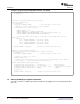
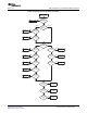
The USB controller provides the following I/O signals. Table 1 shows the USB port pins used in each
mode.
Table 1. USB Pins
Pin Type
(1)
Function
M24XI I Crystal input for M24 oscillator (24 MHZ for USB)
M24X0 O Crystal output for M24 oscillator
M24V
DD
S 1.8V power supply for M24 oscillator
M24V
SS
Ground for M24 oscillator
PLLV
DD18
GND 1.8 Volt power supply for PLLs (system and USB)
USB_VBUS I/O 5V input that signifies that VBUS is connected. The OTG section of the PHY can also pull up or
down on this signal for HNP and SRP.
USB_ID I/O USB_ID is an input that is open or pulled to ground depending on OTG connector configuration.
The state determines if controller starts in HOST or PERIPHERAL mode.
USB_DP I/O USB bi-directional Data Differential signal pair [positive/negative]. Input/output DP signal of the
differential signal pair.
USB_DM I/O USB bi-directional Data Differential signal pair [positive/negative]. Input/output DM signal of the
differential signal pair.
USB_R1 I/O Reference current output. This must be connected via a 10 k Ω 1% resistor to USB_V
SSREF
.
USB_V
SSREF
GND Ground for reference current
USB_V
DDA3P3
S Analog 3.3 V power supply for USB phy
USB_V
SSA3P3
GND Analog ground for USB phy
USB_V
DD1P83
S 1.8 V I/O power supply for USB phy
USB_V
SS1P8
GND I/O Ground for USB phy
USB_V
DDA1P2LDO
S Core Power supply LDO output for USB phy. This must be connected via 1 µ F capacitor to
USB_V
SSA1P2LDO
. Do not connect this to other supply pins.
USB_V
SSA1P2LDO
GND Core Ground for USB phy. This must be connected via 1 µ F capacitor to USB_V
DDA1P2LDO
.
(1)
I = Input, O = Output, Z = High impedance, S = Supply voltage, GND = Ground, A = Analog signal
USB controller provides two mechanism of accessing the endpoint control and status registers:
• Indexed Endpoint Control/Status Registers – These registers are memory-mapped at offset 410h to
41Fh. The endpoint is selected by programming the INDEX register of the controller.
• Non-indexed Endpoint Control/Status Registers – These registers are memory-mapped at offset 500h
to 54Fh. Registers at offset 500h-50Fh map to Endpoint 0; offset 510h-51Fh map to Endpoint 1, and
so on.
For detailed information about the USB controller registers, see Section 4 .
SPRUGH3 – November 2008 Universal Serial Bus (USB) Controller 23
Submit Documentation Feedback