
Digital Media System-on-Chip (DMSoC) Product Preview

www.ti.com
PRODUCT PREVIEW
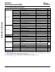
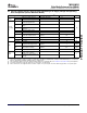
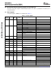
4.3 Electrical Characteristics Over Recommended Ranges of Supply Voltage and Operating
TMS320DM355
Digital Media System-on-Chip (DMSoC)
SPRS463A – SEPTEMBER 2007 – REVISED SEPTEMBER 2007
Case Temperature (Unless Otherwise Noted)
PARAMETER TEST CONDITIONS
(1)
MIN TYP MAX UNIT
V
OH
High-level output voltage
(2)
VDD=MIN, IOH=MAX 2.4
Voltage
V
Output
V
OL
Low-level output voltage
(2)
VDD=MIN, IOL=MAX 0.6
Input current for I/O without
I
I
V
I
= VSS to VDD -1 1
internal pull-up/pull-down
Input current for I/O with internal
I
I(pullup)
V
I
= VSS to VDD 40 190
pull-up
(3) (4)
Current
Input current for I/O with internal
I
I(pulldown)
V
I
= VSS to VDD -190 -40
Input/Outp μ A
pull-down
(3) (4)
ut
I
OH
High-level output current -100
I
OL
Low-level output current 4000
V
O
= VDD or VSS; internal pull
I
OZ
I/O off-state output current ± 10
disabled
C
I
Input capacitance 4
Capacitan
pF
ce
C
O
Output capacitance 4
Resolution Resolution 10 Bits
RLOAD = 499 Ω , Video buffer
INL Integral non-linearity, best fit 1 LSB
disabled
DAC
RLOAD = 499 Ω , Video buffer
DNL Differential non-linearity 0.5 LSB
disabled
Compliance Output compliance range IFS = 1.4 mA, RLOAD = 499 Ω 0 0.700 V
Output high voltage (top of 75%
V
OH(VIDBUF)
1.55
NTSC or PAL colorbar)
(5)
Video
V
Buffer
Outpupt low voltage (bottom of
V
OL(VIDBUF)
0.470
sync tip)
(1) For test conditions shown as MIN, MAX, or NOM, use the appropriate value specified in the recommended operating conditions table.
(2) These I/O specifications apply to regular 3.3 V I/Os and do not apply to DDR2/mDDR, USB I/Os. DDR2/mDDR I/Os are 1.8 V I/Os and
adhere to JESD79-2A standard, USB I/Os adhere to USB2.0 spec.
(3) This specification applies only to pins with an internal pullup (PU) or pulldown (PD). See Section 2.4 or Section 2.5 for pin descriptions.
(4) To pull up a signal to the opposite supply rail, a 1 k Ω resistor is recommended.
(5) 100% color bars are not supported. 100% color bars require 1.2 V peak-to-peak. The video buffer only provides 1.0 V peak-to-peak.
Submit Documentation Feedback Device Operating Conditions 93