
Digital Media System-on-Chip (DMSoC) Product Preview


www.ti.com
PRODUCT PREVIEW
3.9 Pin Multiplexing
3.9.1 Hardware Controlled Pin Multiplexing
TMS320DM355
Digital Media System-on-Chip (DMSoC)
SPRS463A – SEPTEMBER 2007 – REVISED SEPTEMBER 2007
• Power management
– Deep sleep and fast NAND boot control
• Bandwidth Management
– Bus master DMA priority control
For more information on the System Control Module refer to the ARM Subsystem User's Guide.
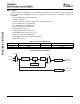
The DM355 makes extensive use of pin multiplexing to accommodate the large number of peripheral
functions in the smallest possible package. In order to accomplish this, pin multiplexing is controlled using
a combination of hardware configuration (at device reset) and software control. No attempt is made by the
DM355 hardware to ensure that the proper pin muxing has been selected for the peripherals or interface
mode being used, thus proper pin muxing configuration is the responsibility of the board and software
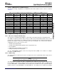
designers. An overview of the pin multiplexing is shown in Table 3-12 .
Table 3-12. Peripheral Pin Mux Overview
Peripheral Muxed With Primary Function Secondary Function Tertiary Function
VPFE (video in) GPIO and SPI2 VPFE (video in) SPI2 GPIO
VPBE (video out) GPIO, PWM, and RTO VPBE (video out) PWM and RTO GPIO
AEMIF GPIO AEMIF GPIO none
ASP0 GPIO ASP0 GPIO none
MMC/SD1 GPIO and UART2 MMC/SD1 GPIO UART2
CLKOUT GPIO CLKOUT GPIO none
I2C GPIO I2C GPIO none
UART1 GPIO UART1 GPIO none
SPI1 GPIO SPI1 GPIO none
SPI0 GPIO SPI0 GPIO none
Use the Asynchronous EMIF configuration pins (AECFG[3:0]) for hardware pin mux control. AECFG[3:0]
control the partitioning of the AEMIF addresses and GPIOs at reset, which allows you to properly
configure the number of AEMIF address pins required by the boot device while unused addresses pins are
available as GPIOs. These settings may be changed by software after reset by programming the PinMux2
register The PinMux2 register is in the System Control Module. As shown in Table 3-13 , the number of
address bits enabled on the AEMIF is selectable from 0 to 16. Pins that are not assigned to another
peripheral and not enabled as address signals become GPIOs (except EM_A[2:1]). The enabled address
signals are always contiguous from EM_BA[1] upwards; bits cannot be skipped. The exception to this are
EM_A[2:1]. These signals (can be used to) represent the ALE and CLE signals for the NAND Flash mode
of the AEMIF and are always enabled. Note that EM_A[0] does not represent the lowest AEMIF address
bit. DM355 supports only 16-bit and 8-bit data widths for the AEMIF. In 16-bit mode, EM_BA[1] represents
the LS address bit (the half-word address) and EM_BA[0] represents the MS address bit (A[14]). In 8-bit
mode, EM_BA[1:0] represent the 2 LS address bits. Note that additional selections are available by
programming the PinMux2 register in software after boot. Note that AECFG selection of ‘0010’ selects
OneNAND interface. The AEMIF needs to operate in the half-rate mode (full_rate = 0) to meet frequency
requirements. Software should not change the PINMUX2 register setting to affect the AEMIF rate
operation. A soft reset of the AEMIF should be performed any time a rate change is made.
Detailed Device Description78 Submit Documentation Feedback