
Digital Media System-on-Chip (DMSoC) Product Preview


www.ti.com
PRODUCT PREVIEW
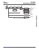
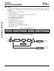
3.6.3 PLLC2
PLLDIV1(/1)
1
0
PLL
0
1
CLKMODE
CLKIN
OSCIN
PLLEN
SYSCLK1
(DDRPHY)
SYSCLKBP
(CLKOUT3)
BPDIV(/8)
PLLM
(programmable)
Pre-DIV
(programmable)
Post-DIV
(/1)
TMS320DM355
Digital Media System-on-Chip (DMSoC)
SPRS463A – SEPTEMBER 2007 – REVISED SEPTEMBER 2007
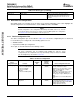
PLLC2 provides the DDR PHY clock and CLKOUT3. Software controls PLLC2 operation through the
PLLC2 registers. The following list, Table 3-11 , and Figure 3-4 describe the customizations of PLLC2 in
the DM355.
• Provides DDR PHY clock and CLKOUT3
• Software configurable
• Accepts clock input or internal oscillator input (same input as PLLC1)
• PLL pre-divider value is programmable
• PLL multiplier value is programmable
• PLL post-divider value is fixed to (/1)
• Only SYSCLK[1] is used
• SYSCLK1 divider value is fixed to (/1)
• SYSCLKBP divider value is fixed to (/8)
• SYSCLK1 is routed to the DDR PHY
• SYSCLKBP is routed to the output pin CLKOUT3
• AUXCLK is not used.
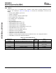
Table 3-11. PLLC2 Output Clocks
Output Clock Used by PLLDIV Divider Notes
SYSCLK1 DDR PHY /1 Fixed divider
SYSCLKBP CLKOUT3 /8 Fixed divider
PLLC2 Configuration in DM355
Detailed Device Description76 Submit Documentation Feedback