
Digital Media System-on-Chip (DMSoC) Product Preview


www.ti.com
PRODUCT PREVIEW
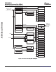
3.2.1 CP15
3.2.2 MMU
3.2.3 Caches and Write Buffer
TMS320DM355
Digital Media System-on-Chip (DMSoC)
SPRS463A – SEPTEMBER 2007 – REVISED SEPTEMBER 2007
• Embedded Trace Module and Embedded Trace Buffer (ETM/ETB)
For more complete details on the ARM9, refer to the ARM926EJ-S Technical Reference Manual, available
at http://www.arm.com
The ARM926EJ-S system control coprocessor (CP15) is used to configure and control instruction and
data caches, Tightly-Coupled Memories (TCMs), Memory Management Unit (MMU), and other ARM
subsystem functions. The CP15 registers are programmed using the MRC and MCR ARM instructions,
when the ARM in a privileged mode such as supervisor or system mode.
The ARM926EJ-S MMU provides virtual memory features required by operating systems such as Linux,
WindowCE, ultron, ThreadX, etc. A single set of two level page tables stored in main memory is used to
control the address translation, permission checks and memory region attributes for both data and
instruction accesses. The MMU uses a single unified Translation Lookaside Buffer (TLB) to cache the
information held in the page tables. The MMU features are:
• Standard ARM architecture v4 and v5 MMU mapping sizes, domains and access protection scheme.
• Mapping sizes are:
– 1MB (sections)
– 64KB (large pages)
– 4KB (small pages)
– 1KB (tiny pages)
• Access permissions for large pages and small pages can be specified separately for each quarter of
the page (subpage permissions)
• Hardware page table walks
• Invalidate entire TLB, using CP15 register 8
• Invalidate TLB entry, selected by MVA, using CP15 register 8
• Lockdown of TLB entries, using CP15 register 10
The size of the Instruction Cache is 16KB, Data cache is 8KB. Additionally, the Caches have the following
features:
• Virtual index, virtual tag, and addressed using the Modified Virtual Address (MVA)
• Four-way set associative, with a cache line length of eight words per line (32-bytes per line) and with
two dirty bits in the Dcache
• Dcache supports write-through and write-back (or copy back) cache operation, selected by memory
region using the C and B bits in the MMU translation tables.
• Critical-word first cache refilling
• Cache lockdown registers enable control over which cache ways are used for allocation on a line fill,
providing a mechanism for both lockdown, and controlling cache corruption
• Dcache stores the Physical Address TAG (PA TAG) corresponding to each Dcache entry in the TAG
RAM for use during the cache line write-backs, in addition to the Virtual Address TAG stored in the
TAG RAM. This means that the MMU is not involved in Dcache write-back operations, removing the
possibility of TLB misses related to the write-back address.
• Cache maintenance operations provide efficient invalidation of, the entire Dcache or Icache, regions of
the Dcache or Icache, and regions of virtual memory.
Submit Documentation Feedback Detailed Device Description 61