
Digital Media System-on-Chip (DMSoC) Product Preview


www.ti.com
PRODUCT PREVIEW
TMS320DM355
Digital Media System-on-Chip (DMSoC)
SPRS463A – SEPTEMBER 2007 – REVISED SEPTEMBER 2007
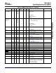
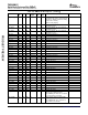
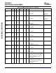
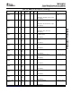
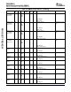
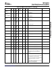
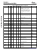
Table 2-23. DM355 Pin Descriptions (continued)
Name BGA Type Group Power PU Reset Description
(4)
Mux Control
ID
(1)
Supply
(2)
PD
(3)
State
DDR_VREF U10 PWR DDRI V
DD_DDR
DDR: Voltage input for the SSTL_18 IO
O buffers
V
SSA_DLL
R11 GND DDRD V
DD_DDR
DDR: Ground for the DDR DLL
LL
V
DDA33_DDRDLL
R10 PWR DDRD V
DD_DDR
DDR: Power (3.3 Volts) for the DDR DLL
LL
DDR_ZN T9 I/O DDRI V
DD_DDR
DDR: Reference output for drive strength
O calibration of N and P channel outputs. Tie
to ground via 50 ohm resistor @ 0.5%
tolerance.
EM_A13 / V19 I/O AEMI V
DD
PD in L Async EMIF: Address Bus bit[13] PINMUX2[0].EM_A1
GIO067 / F / 3_3,
BTSEL[1] GIO /
syste
m
GIO: GIO[067] default set by
AECFG[0]
System: BTSEL[1:0] sampled at
Power-on-Reset to determine Boot method
(00:NAND, 01:Flash, 10:UART, 11:SD)
EM_A12 / U19 I/O AEMI V
DD
PD in L Async EMIF: Address Bus bit[12] PINMUX2[0].EM_A1
GIO066 / F / 3_3,
BTSEL[0] GIO /
syste
m
GIO: GIO[066] default set by
AECFG[0]
System: BTSEL[1:0] sampled at
Power-on-Reset to determine Boot method
(00:NAND, 01:Flash, 10:UART, 11:SD)
EM_A11 / R16 I/O AEMI V
DD
PU in H Async EMIF: Address Bus bit[11] PINMUX2[0].EM_A1
GIO065 / F / 3_3,
AECFG[3] GIO /
syste
m
GIO: GIO[065] default set by
AECFG[0]
System: AECFG[3:0] sampled at
Power-on-Reset to set AEMIF Configuration
AECFG[3] sets default for
PinMux2.EM_D15_8: AEMIF Default Bus
Width (0:16 or 1:8 bits)
EM_A10 / R18 I/O AEMI V
DD
PU in H Async EMIF: Address Bus bit[10] PINMUX2[0].EM_A1
GIO064 / F / 3_3,
AECFG[2] GIO /
syste
m
GIO: GIO[064] default set by
AECFG[0]
System: AECFG[3:0] sampled at
Power-on-Reset to set AEMIF Configuration
AECFG[2:1] sets default for
PinMux2.EM_BA0: AEMIF EM_BA0
Definition (00: EM_BA0, 01: EM_A14,
10:GIO[054], 11:rsvd)
Submit Documentation Feedback Device Overview 43