
Digital Media System-on-Chip (DMSoC) Product Preview


www.ti.com
PRODUCT PREVIEW
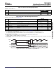
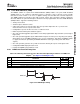
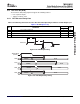
Bit0 Bit(n-1) (n-2) (n-3) (n-4)
Bit0 Bit(n-1) (n-2) (n-3) (n-4)
M50
M49
M45
M46
M44
M43
CLKX
FSX
DX
DR
M52
TMS320DM355
Digital Media System-on-Chip (DMSoC)
SPRS463A – SEPTEMBER 2007 – REVISED SEPTEMBER 2007
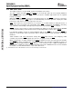
Table 5-41. ASP as SPI Timing Requirements
CLKSTP = 10b, CLKXP = 1 (see Figure 5-44 )
MASTER
NO. UNIT
MIN MAX
M49 t
su(DRV-CKXH)
Setup time, DR valid before CLKX high 11 ns
M50 t
h(CKXH-DRV)
Hold time, DR valid after CLKX high 0 ns
Table 5-42. ASP as SPI Switching Characteristics
(1) (2)
CLKSTP = 10b, CLKXP = 1 (see Figure 5-44 )
MASTER
NO. PARAMETER UNIT
MIN MAX
38.5 or
M52 tc(CKX) Cycle time, CLKX ns
2P
(1) (3)
M43 t
d(CKXH-FXH)
Delay time, CLKX high to FSX high
(4)
T – 1 T + 3 ns
M44 t
d(FXL-CKXL)
Delay time, FSX low to CLKX low
(5)
D – 2 D + 2 ns
M45 t
d(CKXL-DXV)
Delay time, CLKX low to DX valid –2 6 ns
Disable time, DX high impedance following last data bit from
M46 t
dis(CKXH-DXHZ)
D – 3 D + 3 ns
CLKX high
(1) P = (1/SYSCLK2), where SYSCLK2 is an output clock of PLLC1 (see Section 3.5 ) .
(2) T = CLKX period = (1 + CLKGDV) × P
C = CLKX low pulse width = T/2 when CLKGDV is odd or zero and = (CLKGDV/2) × P when CLKGDV is even
D = CLKX high pulse width = T/2 when CLKGDV is odd or zero and = (CLKGDV/2 + 1) × P when CLKGDV is even
(3) Use which ever value is greater.
(4) FSRP = FSXP = 1. As a SPI master, FSX is inverted to provide active-low slave-enable output.
CLKXM = FSXM = 1, CLKRM = FSRM = 0 for master ASP
(5) FSX should be low before the rising edge of clock to enable slave devices and then begin a SPI transfer at the rising edge of the master
clock (CLKX).
Figure 5-44. ASP as SPI: CLKSTP = 10b, CLKXP = 1
142 Peripheral Information and Electrical Specifications Submit Documentation Feedback