
Digital Media System-on-Chip (DMSoC) Product Preview

www.ti.com
PRODUCT PREVIEW
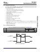
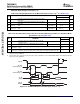
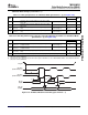
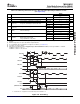
Bit(n-1) (n-2) (n-3)
Bit0 Bit(n-1) (n-2) (n-3)
14
11
10
9
3
3
2
8
6
5
4
4
13
(A)
13
(A)
A. ParameterNo.13appliestothefirstdatabitonly whenXDATDLY ≠ 0.
CLKR
FSR(int)
FSR(ext)
DR
CLKX
FSX(int)
FSX(ext)
FSX
(XDATDLY=00b)
DX
15
CLKS
16
16
17
17
3
2
3
7
12
TMS320DM355
Digital Media System-on-Chip (DMSoC)
SPRS463A – SEPTEMBER 2007 – REVISED SEPTEMBER 2007
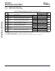
Table 5-36. Switching Characteristics Over Recommended Operating Conditions for ASP
(1) (2)
(see Figure 5-41 )
DM355
NO. PARAMETER UNIT
MIN MAX
2 t
c(CKRX)
Cycle time, CLKR/X CLKR/X int 38.5 or 2P
(3) (4)
ns
17 td(CLKS-CLKRX) Delay time, CLKS high to internal CLKR/X CLKR/X int 1 24
3 t
w(CKRX)
Pulse duration, CLKR/X high or CLKR/X low CLKR/X int C - 1 C + 1 ns
CLKR int 3 25
4 t
d(CKRH-FRV)
Delay time, CLKR high to internal FSR valid ns
CLKR ext 3 25
CLKX int -4 8
9 t
d(CKXH-FXV)
Delay time, CLKX high to internal FSX valid ns
CLKX ext 3 25
CLKX int 12 ns
tdis(CKXH- Disable time, DX high impedance following last data
12
DXHZ) bit from CLKX high
CLKX ext 12 ns
CLKX int -5 12 ns
13 t
d(CKXH-DXV)
Delay time, CLKX high to DX valid
CLKX ext 3 25 ns
Delay time, FSX high to DX valid FSX int 14
(5)
14 t
d(FXH-DXV)
ONLY applies when in data ns
FSX ext 25
(5)
delay 0 (XDATDLY = 00b) mode
(1) CLKRP = CLKXP = FSRP = FSXP = 0. If polarity of any of the signals is inverted, then the timing references of that signal are also
inverted.
(2) Minimum delay times also represent minimum output hold times.
(3) P = (1/SYSCLK2), where SYSCLK2 is an output clock of PLLC1 (see Section 3.5 ) .
(4) Use which ever value is greater.
(5) Extra delay from FSX high to DX valid applies only to the first data bit of a device, if and only if DXENA = 1 in SPCR.
if DXENA = 0, then D1 = D2 = 0
if DXENA = 1, then D1 = 4P, D2 = 8P
Figure 5-41. ASP Timing
Submit Documentation Feedback Peripheral Information and Electrical Specifications 139