
Digital Media System-on-Chip (DMSoC) Product Preview

www.ti.com
PRODUCT PREVIEW
5.12 Serial Port Interface (SPI)
5.12.1 SPI Electrical Data/Timing
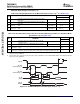
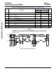
SPIx_CLK
(ClockPolarity=0)
1
2
3
SPIx_CLK
(ClockPolarity=1)
TMS320DM355
Digital Media System-on-Chip (DMSoC)
SPRS463A – SEPTEMBER 2007 – REVISED SEPTEMBER 2007
The contains 3 separate SPI modules. These modules provide a programmable length shift register which
allows serial communication with other SPI devices through a 3 or 4 wire interface (Clock, Data In, Data
Out, and Enable). The SPI supports the following features:
• Master mode operation
• 2 chip selects for interfacing to multiple slave SPI devices.
• 3 or 4 wire interface (Clock, Data In, Data Out, and Enable)
• Unique interrupt for each SPI port
• Separate DMA events for SPI Receive and Transmit
• 16-bit shift register
• Receive buffer register
• Programmable character length (2 to 16 bits)
• Programmable SPI clock frequency range
• 8-bit clock prescaler
• Programmable clock phase (delay or no delay)
• Programmable clock polarity
The SPI modules do not support the following features:
• Slave mode. Only Master mode is supported in DM355 (Master mode means that DM355 provides the
serial clock).
• GPIO mode. GPIO functionality is supported by the GIO modules for those SPI pins that are
multiplexed with GPIO signals.
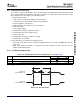
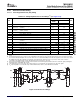
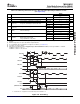
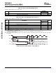
Table 5-28. Timing Requirements for SPI (All Modes)
(1)
(see Figure 5-36 )
DM355
NO. UNIT
MIN MAX
1 t
c(CLK)
Cycle time, SPI_CLK 37. 037 ns ns
2 t
w(CLKH)
Pulse duration, SPI_CLK high (All Master Modes) 0.45*T 0.55*T ns
3 t
w(CLKL)
Pulse duration, SPI_CLK low (All Master Modes 0.45*T 0.55*T ns
(1) T = t
c(CLK)
= SPI_CLK period is equal to the SPI module clock divided by a configurable divider.
Figure 5-36. SPI_CLK Timing
Submit Documentation Feedback Peripheral Information and Electrical Specifications 131