
Digital Media System-on-Chip (DMSoC) Product Preview

www.ti.com
PRODUCT PREVIEW
5.10 USB 2.0
5.10.1 USB2.0 Electrical Data/Timing
TMS320DM355
Digital Media System-on-Chip (DMSoC)
SPRS463A – SEPTEMBER 2007 – REVISED SEPTEMBER 2007
DM355 includes a USB Controller Module that is built around the Mentor USB Multi-Point High-Speed
Dual Role Controller, endpoint memory, CPPI DMA controller and UTMI+ PHY. The controller conforms to
USB 2.0 Specification. The USB2.0 peripheral supports the following features:
• USB 2.0 peripheral at speeds high speed (HS: 480 Mb/s) and full speed (FS: 12 Mb/s)
• USB 2.0 host at speeds HS, FS, and low speed (LS: 1.5 Mb/s)
• All transfer modes (control, bulk, interrupt, and isochronous)
• Four Transmit (TX) and four Receive (RX) endpoints in addition to endpoint 0
• FIFO RAM
– 4K endpoint
– Programmable FIFO size
• Connects to a standard UTMI+ PHY with a 60 MHz, 8-bit interface
• Includes a DMA sub-module that supports four TX and four RX channels of CPPI 3.0 DMAs
• RNDIS mode for accelerating RNDIS type protocols using short packet termination over USB
• USB OTG extensions, i.e. session request protocol (SRP) and host negotiation protocol (HNP)
The USB2.0 peripheral does not support the following features:
• On-chip charge pump
• High bandwidth ISO mode is not supported (triple buffering)
• 16-bit 30 MHz UTMI+ interface is not supported
• RNDIS mode acceleration for USB sizes that are not multiples of 64 bytes
• Endpoint max USB packet sizes that do not conform to the USB 2.0 spec (for FS/LS: 8, 16, 32, 64,
and 1023 are defined; for HS: 64, 128, 512, and 1024 are defined)
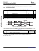
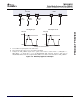
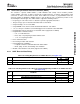
Table 5-25. Switching Characteristics Over Recommended Operating Conditions for USB2.0 (see
Figure 5-33 )
DM355
LOW SPEED FULL SPEED HIGH SPEED
(1)
NO. PARAMETER UNIT
1.5 Mbps 12 Mbps 480 Mbps
MIN MAX MIN MAX MIN MAX
1 t
r(D)
Rise time, USB_DP and USB_DM signals
(2)
75 300 4 20 0.5 ns
2 t
f(D)
Fall time, USB_DP and USB_DM signals
(2)
75 300 4 20 0.5 ns
3 t
frfm
Rise/Fall time, matching
(3)
80 125 90 111.11 %
4 V
CRS
Output signal cross-over voltage
(2)
1.3 2 1.3 2 V
5 t
jr(source)NT
Source (Host) Driver jitter, next transition 2 2 ns
t
jr(FUNC)NT
Function Driver jitter, next transition 25 2 ns
6 t
jr(source)PT
Source (Host) Driver jitter, paired transition
(4)
1 1 ns
t
jr(FUNC)PT
Function Driver jitter, paired transition 10 1 ns
7 t
w(EOPT)
Pulse duration, EOP transmitter 1250 1500 160 175 ns
8 t
w(EOPR)
Pulse duration, EOP receiver 670 82 ns
9 t
(DRATE)
Data Rate 1.5 12 480 Mb/s
10 Z
DRV
Driver Output Resistance – – 28 49.5 40.5 49.5 Ω
(1) For more detailed specification information, see the Universal Serial Bus Specification Revision 2.0, Chapter 7. Electrical.
(2) Low Speed: C
L
= 200 pF, Full Speed: C
L
= 50 pF, High Speed: C
L
= 50 pF
(3) t
frfm
= (t
r
/t
f
) x 100. [Excluding the first transaction from the Idle state.]
(4) t
jr
= t
px(1)
- t
px(0)
Submit Documentation Feedback Peripheral Information and Electrical Specifications 127