
Digital Media System-on-Chip (DMSoC) Product Preview

www.ti.com
PRODUCT PREVIEW
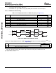
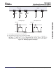
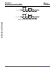
DIN<9:0>
DACDigitalInput
C
BG
0.1 Fm
VREF
VideoDACandBuffer
R
BIAS
2550 Ω
IBIAS
R
fb
= 1000 Ω
IOUT VFB TVOUT
R
out
=1070 Ω
TVmonitor
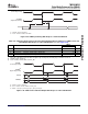
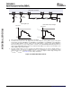
TVOUT[V]
VideoBufferOutputVoltage
MSB
LSB
V
OL(VIDBUF)
V
OH(VIDBUF)
0
TMS320DM355
Digital Media System-on-Chip (DMSoC)
SPRS463A – SEPTEMBER 2007 – REVISED SEPTEMBER 2007
A. Place capacitors and resistors as close as possible to the DM355.
B. You must use the circuit shown in this diagram. Also you must configure the VDAC_CONFIG register in the System
Control module as follows: TRESB4R4 = 0x3, TRESB4R2 = 0x8, TRESB4R1 = 0x8, TRIMBITS = 0x34, PWD_BGZ =
1 (power up VREF), SPEED = 1 (faster), TVINT = don't care, PWD_VBUFZ = 1 (power up video buffer), VREFSET =
don't care, ACCUP_EN = 0 (no A/C coupling), DINV = 1 (invert). See the TMS320DM355 ARM Subsystem Reference
Guide and the TMS320DM355 DMSoC Video Processing Back End (VPBE) User's Guide for more information on the
VDAC_CONFIG register and Video Buffer.
C. For proper TVOUT voltage, you must connect the pin TVOUT directly to the TV. No A/C coupling capacitor or
termination resistor is necessary on your DM355 board. Also, it is assumed that the TV has no internal A/C coupling
capacitor but does have an internal termination resistor, as shown in this diagram. TVOUT voltage will range from
V
OL(VIDBUF)
to V
OH(VIDBUF)
. See Section 4.3 for the voltage specifications.
Figure 5-32. DAC With Buffer Circuit
126 Peripheral Information and Electrical Specifications Submit Documentation Feedback