
Digital Media System-on-Chip (DMSoC) Product Preview

www.ti.com
PRODUCT PREVIEW
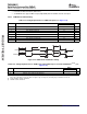
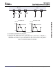
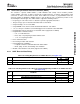
VCLKIN
(A)
(Positive Edge Clocking)
9
VCLKIN
(A)
(Negative Edge Clocking)
10
VCTL
(B)
A. VCLKIN=PCLKorEXTCLK
B. VCTL=HSYNC,VSYNC,andFIELD
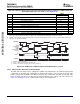
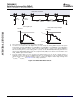
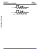
VCLKIN
(A)
(Positive Edge Clocking)
13
VCLKIN
(A)
(Negative Edge Clocking)
11
VCTL
(B)
A. VCLKIN=PCLKorEXTCLK
B. VCTL=HSYNC,VSYNC,FIELD,andLCD_OE
C. VDATA=COUT[7:0],YOUT[7:0],R[7:3],G[7:2],andB[7:3]
VDATA
(C)
14
12
TMS320DM355
Digital Media System-on-Chip (DMSoC)
SPRS463A – SEPTEMBER 2007 – REVISED SEPTEMBER 2007
Figure 5-28. VPBE Input Timing With Respect to PCLK and EXTCLK
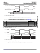
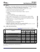
Table 5-23. Switching Characteristics Over Recommended Operating Conditions for VPBE Control and
Data Output With Respect to PCLK and EXTCLK
(1) (2) (3)
(see Figure 5-29 )
DM355
NO. PARAMETER UNIT
MIN MAX
11 t
d(VCLKIN-VCTLV)
Delay time, VCLKIN edge to VCTL valid 13.3 ns
12 t
d(VCLKIN-VCTLIV)
Delay time, VCLKIN edge to VCTL invalid 2 ns
13 t
d(VCLKIN-VDATAV)
Delay time, VCLKIN edge to VDATA valid 13.3 ns
14 t
d(VCLKIN-VDATAIV)
Delay time, VCLKIN edge to VDATA invalid 2 ns
(1) The VPBE may be configured to operate in either positive or negative edge clocking mode. When in positive edge clocking mode, the
rising edge of VCLKIN is referenced. When in negative edge clocking mode, the falling edge of VCLKIN is referenced.
(2) VCLKIN = PCLK or EXTCLK
(3) VCTL = HSYNC, VSYNC, FIELD, and LCD_OE
Figure 5-29. VPBE Control and Data Output With Respect to PCLK and EXTCLK
Submit Documentation Feedback Peripheral Information and Electrical Specifications 123