
Stereo System User Manual

www.ti.com
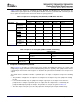
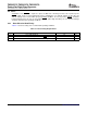
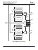
4.4 Electrical Characteristics
TMS320C6727, TMS320C6726, TMS320C6722
Floating-Point Digital Signal Processors
SPRS268E – MAY 2005 – REVISED JANUARY 2007
Over Operating Case Temperature Range (Unless Otherwise Noted)
PARAMETER TEST CONDITIONS MIN TYP MAX UNIT
V
OH
High Level Output Voltage I
O
= –100 µA DV
DD
– 0.2 V
V
OL
Low Level Output Voltage I
O
= 100 µA 0.2 V
I
OH
High-Level Output Current V
O
= 0.8 DV
DD
–8 mA
I
OL
Low-Level Output Current V
O
= 0.22 DV
DD
8 mA
V
IH
High-Level Input Voltage 2 DV
DD
V
V
IL
Low-Level Input Voltage 0 0.8 V
V
HYS
Input Hysterisis 0.13 DV
DD
V
I
I
, I
OZ
Input Current and Off State Output Pins without pullup or pulldown ± 10
Current
Pins with internal pullup –50 –170 µA
Pins with internal pulldown 50 170
t
tr
Input Transition Time 25 ns
C
I
Input Capacitance 7 pF
C
O
Output Capacitance 7 pF
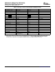
I
DD2V
CV
DD
Supply
(1)
GDH, CV
DD
= 1.2 V, 658
CPU clock = 300 MHz
mA
RFP, CV
DD
= 1.2 V, 555
CPU clock = 250 MHz
I
DD3V
DV
DD
Supply
(1)
GDH, DV
DD
= 3.3 V, 76
32-bit EMIF speed = 100 MHz
mA
RFP, DV
DD
= 3.3 V, 58
16-bit EMIF speed = 100 MHz
(1) Assumes the following conditions: 25 ° C case temperature; 60% CPU utilization; EMIF at 50% utilization (100 MHz), 50% writes, (32 bits
for GDH, 16 bits for RFP), 50% bit switching; two 10-MHz SPI at 100% utilization, 50% bit switching.
The actual current draw is highly application-dependent. For more details on core and I/O activity, refer to the TMS320C672x Power
Consumption Summary Application Report (literature number SPRAAA4 ).
34 Peripheral and Electrical Specifications Submit Documentation Feedback