
Stereo System User Manual

www.ti.com
TMS320C6727, TMS320C6726, TMS320C6722
Floating-Point Digital Signal Processors
SPRS268E – MAY 2005 – REVISED JANUARY 2007
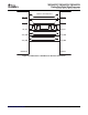
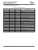
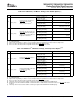
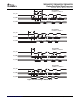
Table 4-27. Additional
(1)
SPI Master Timings, 4-Pin Enable Option
(2) (3)
NO. MIN MAX UNIT
Polarity = 0, Phase = 0,
3P + 15
to SPIx_CLK rising
Polarity = 0, Phase = 1,
0.5t
c(SPC)M
+ 3P + 15
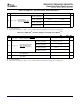
Delay from slave assertion of
to SPIx_CLK rising
17 t
d(ENA_SPC)M
SPIx_ENA active to first ns
Polarity = 1, Phase = 0,
SPIx_CLK from master.
(4)
3P + 15
to SPIx_CLK falling
Polarity = 1, Phase = 1,
0.5t
c(SPC)M
+ 3P + 15
to SPIx_CLK falling
Polarity = 0, Phase = 0,
0.5t
c(SPC)M
from SPIx_CLK falling
Polarity = 0, Phase = 1,
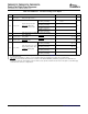
Max delay for slave to deassert
0
from SPIx_CLK falling
SPIx_ENA after final SPIx_CLK
18 t
d(SPC_ENA)M
ns
edge to ensure master does not
Polarity = 1, Phase = 0,
0.5t
c(SPC)M
begin the next transfer.
(5)
from SPIx_CLK rising
Polarity = 1, Phase = 1,
0
from SPIx_CLK rising
(1) These parameters are in addition to the general timings for SPI master modes (Table 4-25 ).
(2) P = SYSCLK2 period
(3) Figure shows only Polarity = 0, Phase = 0 as an example. Table gives parameters for all four master clocking modes.
(4) In the case where the master SPI is ready with new data before SPIx_ENA assertion.
(5) In the case where the master SPI is ready with new data before SPIx_ENA deassertion.
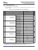
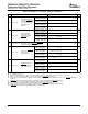
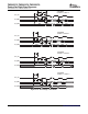
Table 4-28. Additional
(1)
SPI Master Timings, 4-Pin Chip Select Option
(2) (3)
NO. MIN MAX UNIT
Polarity = 0, Phase = 0,
2P – 10
to SPIx_CLK rising
Polarity = 0, Phase = 1,
0.5t
c(SPC)M
+ 2P – 10
to SPIx_CLK rising
Delay from SPIx_SCS active to
19 t
d(SCS_SPC)M
ns
first SPIx_CLK
(4) (5)
Polarity = 1, Phase = 0,
2P – 10
to SPIx_CLK falling
Polarity = 1, Phase = 1,
0.5t
c(SPC)M
+ 2P – 10
to SPIx_CLK falling
Polarity = 0, Phase = 0,
0.5t
c(SPC)M
from SPIx_CLK falling
Polarity = 0, Phase = 1,
0
Delay from final SPIx_CLK edge
from SPIx_CLK falling
20 t
d(SPC_SCS)M
to master deasserting ns
Polarity = 1, Phase = 0,
SPIx_SCS
(6) (7)
0.5t
c(SPC)M
from SPIx_CLK rising
Polarity = 1, Phase = 1,
0
from SPIx_CLK rising
(1) These parameters are in addition to the general timings for SPI master modes (Table 4-25 ).
(2) P = SYSCLK2 period
(3) Figure shows only Polarity = 0, Phase = 0 as an example. Table gives parameters for all four master clocking modes.
(4) In the case where the master SPI is ready with new data before SPIx_SCS assertion.
(5) This delay can be increased under software control by the register bit field SPIDELAY.C2TDELAY[4:0].
(6) Except for modes when SPIDAT1.CSHOLD is enabled and there is additional data to transmit. In this case, SPIx_SCS will remain
asserted.
(7) This delay can be increased under software control by the register bit field SPIDELAY.T2CDELAY[4:0].
Submit Documentation Feedback Peripheral and Electrical Specifications 85