
Stereo System User Manual

www.ti.com
TMS320C6727, TMS320C6726, TMS320C6722
Floating-Point Digital Signal Processors
SPRS268E – MAY 2005 – REVISED JANUARY 2007
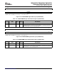
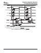
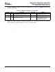
31 8
Reserved
7 0
HPIAMSB
R/W, 0
LEGEND: R/W = Read/Write; R = Read only; - n = value after reset
Figure 4-19. CFGHPIAMSB Register Bit Layout (0x4000 000C)
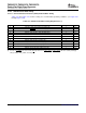
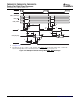
Table 4-13. CFGHPIAMSB Register Bit Field Description (0x4000 000C)
RESET READ
BIT NO. NAME DESCRIPTION
VALUE WRITE
31:8 Reserved N/A N/A Reads are indeterminate. Only 0s should be written to these bits.
7:0 HPIAMSB 0 R/W UHPI most significant byte of DSP address to access in Non-Multiplexed mode and
in Multiplexed Address and Data mode when PAGEM = 1. Sets bits [31:24] of the
DSP internal address as accessed through UHPI.
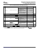
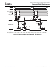
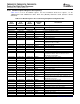
31 8
Reserved
7 0
HPIAUMB
R/W, 0
LEGEND: R/W = Read/Write; R = Read only; - n = value after reset
Figure 4-20. CFGHPIAUMB Register Bit Layout (0x4000 0010)
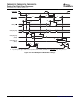
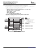
Table 4-14. CFGHPIAUMB Register Bit Field Description (0x4000 0010)
RESET READ
BIT NO. NAME DESCRIPTION
VALUE WRITE
31:8 Reserved N/A N/A Reads are indeterminate. Only 0s should be written to these bits.
7:0 HPIAUMB 0 R/W UHPI upper middle byte of DSP address to access in Non-Multiplexed mode and in
Multiplexed Address and Data mode when PAGEM = 1. Sets bits [23:16] of the DSP
internal address as accessed through UHPI.
Submit Documentation Feedback Peripheral and Electrical Specifications 61