
Stereo System User Manual

www.ti.com
TMS320C6727, TMS320C6726, TMS320C6722
Floating-Point Digital Signal Processors
SPRS268E – MAY 2005 – REVISED JANUARY 2007
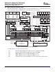
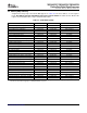
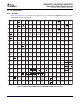
Figure 2-6 shows the bit layout of the CFGPIN0 register and Table 2-10 contains a description of the bits.
31 8
Reserved
7 6 5 4 3 2 1 0
PINCAP7 PINCAP6 PINCAP5 PINCAP4 PINCAP3 PINCAP2 PINCAP1 PINCAP0
LEGEND: R/W = Read/Write; R = Read only; - n = value after reset
Figure 2-6. CFGPIN0 Register Bit Layout (0x4000 0000)
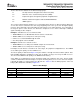
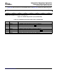
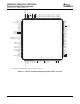
Table 2-10. CFGPIN0 Register Bit Field Description (0x4000 0000)
BIT NO. NAME DESCRIPTION
31:8 Reserved Reads are indeterminate. Only 0s should be written to these bits.
7 PINCAP7 SPI0_SOMI/I2C0_SDA pin state captured on rising edge of RESET pin.
6 PINCAP6 SPI0_SIMO pin state captured on rising edge of RESET pin.
5 PINCAP5 SPI0_CLK/I2C0_SCL pin state captured on rising edge of RESET pin.
4 PINCAP4 SPI0_SCS/I2C1_SCL pin state captured on rising edge of RESET pin.
3 PINCAP3 SPI0_ENA/I2C1_SDA pin state captured on rising edge of RESET pin.
2 PINCAP2 AXR0[8]/AXR1[5]/SPI1_SOMI pin state captured on rising edge of RESET pin.
1 PINCAP1 AXR0[9]/AXR1[4]/SPI1_SIMO pin state captured on rising edge of RESET pin.
0 PINCAP0 AXR0[7]/SPI1_CLK pin state captured on rising edge of RESET pin.
Submit Documentation Feedback Device Overview 17