
Interpolated Control (VIC) Port Reference Guide


GPIO Registers
5-15General Purpose I/O OperationSPRU629
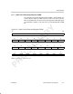
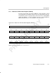
5.1.7 Video Port Pin Data Set Register (PDSET)
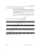
The video port pin data set register (PDSET) is shown in Figure 5–7 and
described in Table 5–8. PDSET is an alias of the video port pin data output reg-
ister (PDOUT) for writes only and provides an alternate means of driving GPIO
outputs high. Writing a 1 to a bit of PDSET sets the corresponding bit in
PDOUT. Writing a 0 has no effect. Register reads return all 0s.
Figure 5–7. Video Port Pin Data Set Register (PDSET)
31 24
Reserved
R-0
23 22 21 20 19 18 17 16
Reserved PDSET22 PDSET21 PDSET20 PDSET19 PDSET18 PDSET17 PDSET16
R-0 W-0 W-0 W-0 W-0 W-0 W-0 W-0
15 14 13 12 11 10 9 8
PDSET15 PDSET14 PDSET13 PDSET12 PDSET11 PDSET10 PDSET9 PDSET8
W-0 W-0 W-0 W-0 W-0 W-0 W-0 W-0
76543210
PDSET7 PDSET6 PDSET5 PDSET4 PDSET3 PDSET2 PDSET1 PDSET0
W-0 W-0 W-0 W-0 W-0 W-0 W-0 W-0
Legend: R = Read only; W = Write only; -n = value after reset