
Interpolated Control (VIC) Port Reference Guide


GPIO Registers
General Purpose I/O Operation5-12 SPRU629
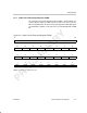
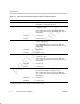
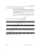
Table 5–6. Video Port Pin Data Input Register (PDIN) Field Descriptions
Bit field
†
symval
†
Value Description
31–23 Reserved – 0 Reserved. The reserved bit location is always read as 0. A
value written to this field has no effect.
22 PDIN22 PDIN22 bit returns the logic level of the VCTL3 pin.
VCTL3LO 0 Pin is logic low.
VCTL3HI 1 Pin is logic high.
21
PDIN21 PDIN21 bit returns the logic level of the VCTL2 pin.
VCTL2LO 0 Pin is logic low.
VCTL2HI 1 Pin is logic high.
20
PDIN20 PDIN20 bit returns the logic level of the VCTL1 pin.
VCTL1LO 0 Pin is logic low.
VCTL1HI 1 Pin is logic high.
19–0
PDIN[19–0] PDIN[19–0] bit returns the logic level of the corresponding
VDATA[n] pin.
VDATAnLO 0 Pin is logic low.
VDATAnHI 1 Pin is logic high.
†
For CSL implementation, use the notation VP_PDIN_PDINn_symval