
Interpolated Control (VIC) Port Reference Guide


Video Display Registers
4-87Video Display PortSPRU629
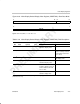
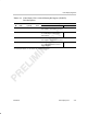
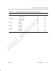
Figure 4–63. Video Display Default Display Value Register (VDDEFVAL)—Raw Data Mode
31 20 19 16
Reserved
DEFVAL
R/W-0 R/W-0
15 0
DEFVAL
R/W-0
Legend: R/W = Read/Write; -n = value after reset
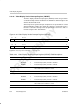
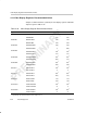
Table 4–29. Video Display Default Display Value Register (VDDEFVAL) Field Descriptions
Description
Bit field
†
symval
†
Value
BT.656 and Y/C Mode
Raw Data Mode
31–24 CRDEFVAL OF(value) 0–FFh Specifies the 8 MSBs of the
default Cr display value.
Not used.
31–20
‡
Reserved – 0 Not used. Reserved. The reserved bit
location is always read as 0.
A value written to this field
has no effect.
19–0
‡
DEFVAL OF(value) 0–FFFFFh Not used. Specifies the default raw
data display value.
23–16 CBDEFVAL OF(value) 0–FFh Specifies the 8 MSBs of the
default Cb display value.
Not used.
15–8 Reserved – 0 Reserved. The reserved bit
location is always read as 0.
A value written to this field
has no effect.
Not used.
7–0 YDEFVAL OF(value) 0–FFh Specifies the 8 MSBs of the
default Y display value.
Not used.
†
For CSL implementation, use the notation VP_VDDEFVAL_field_symval
‡
Raw data mode only.