
Interpolated Control (VIC) Port Reference Guide

Video Display Registers
4-55Video Display PortSPRU629
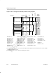
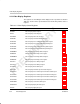
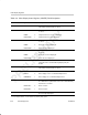
4.12.2 Video Display Control Register (VDCTL)
The video display is controlled by the video display control register (VDCTL).
The VDCTL is shown in Figure 4–40 and described in Table 4–7.
Figure 4–40. Video Display Control Register (VDCTL)
31 30 29 28 27 24
RSTCH
BLKDIS Reserved PVPSYN Reserved
R/WS-0 R/W-1 R-0 R/W-0 R-0
23 22 21 20 19 18 17 16
FXS
VXS HXS VCTL3S VCTL2S VCTL1S
R/W-0 R/W-0 R/W-0 R/W-0 R/W-0 R/W-0
15 14 13 12 11 10 9 8
VDEN
DPK RGBX RSYNC DVEN RESMPL Reserved SCALE
R/W-0 R/W-0 R/W-0 R/W-0 R/W-0 R/W-0 R-0 R/W-0
765432 0
CON
FRAME DF2 DF1 Reserved DMODE
R/W-0 R/W-0 R/W-0 R/W-0 R-0 R/W-0
Legend: R = Read only; R/W = Read/Write; WS = Write 1 to reset, write of 0 has no effect; -n = value after reset
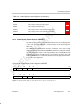
Table 4–7. Video Display Control Register (VDCTL) Field Descriptions
Description
Bit field
†
symval
†
Value
BT.656 and Y/C Mode
Raw Data Mode
31 RSTCH Reset channel bit. Write 1 to reset the bit, a write of 0 has no effect.
NONE 0 No effect.
RESET 1 Resets the video display module and sets its registers to their
initial values. Also clears the VDEN bit. The video display module
automatically clears RSTCH after software reset is completed.
†
For CSL implementation, use the notation VP_VDCTL_field_symval
‡
For complete encoding of these bits, see Table 4–4.