
Interpolated Control (VIC) Port Reference Guide


Video Capture FIFO Registers
3-83Video Capture PortSPRU629
3.14 Video Capture FIFO Registers
The capture FIFO mapping registers are listed in Table 3–34. These registers
provide read access to the capture FIFOs. These pseudo-registers should be
mapped into DSP memory space rather than configuration register space in
order to provide high-speed access. See the device-specific datasheet for the
memory address of these registers. The function of the video capture FIFO
mapping registers is listed in Table 3–35.
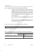
Table 3–34. Video Capture FIFO Registers
Acronym Register Name
YSRCA Y FIFO Source Register A
CBSRCA Cb FIFO Source Register A
CRSRCA Cr FIFO Source Register A
YSRCB Y FIFO Source Register B
CBSRCB Cb FIFO Source Register B
CRSRCB
Cr FIFO Source Register B
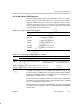
Table 3–35. Video Capture FIFO Registers Function
Capture Mode
Register
BT.656 or Y/C
Raw Data TSI
YSRCx Maps Y capture buffer into DSP memory. Maps data capture buffer
into the DSP memory.
Maps data capture buffer
into the DSP memory.
CBSRCx Maps Cb capture buffer into DSP memory. Not used. Not used.
CRSRCx
Maps Cr capture buffer into DSP memory. Not used. Not used.
In BT.656 or Y/C capture mode, three DMAs move data from the Y, Cb, and
Cr capture FIFOs to the DSP memory by using the memory-mapped YSRCx,
CBSRCx, and CRSRCx registers. The DMA transfers are triggered by the
YEVT, CbEVT, and CrEVT events, respectively.
In raw capture mode, one DMA channel moves data from the Y capture FIFO
to the DSP memory by using the memory-mapped YSRCx register. The DMA
transfers are triggered by a YEVT event.
The video port packs receive data into 64-bit words in the FIFO and the DMA
should always move 64-bit-wide data from YSRCx, CBSRCx, and CRSRCx
to the memory.