
- TMS320C645x General-Purpose Input/Output SPRU724 User's Guide

Registers
19General-Purpose Input/Output (GPIO)SPRU724
5.4 Set Data Register (SET_DATA)
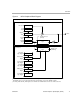
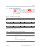
The GPIO set data register (SET_DATA) is shown in Figure 6 and described
in Table 6. SET_DATA provides an alternate means of driving GPIO outputs
high. Writing a 1 to a bit of SET_DATA sets the corresponding bit in
OUT_DATA. Writing a 0 has no effect. Reading SET_DATA returns the
contents of OUT_DATA.
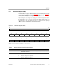
Figure 6. Set Data Register (SET_DATA)
31 16
Reserved
R-0
15 14 13 12 11 10 9 8
SET15 SET14 SET13 SET12 SET11 SET10 SET9 SET8
R/W-0 R/W-0 R/W-0 R/W-0 R/W-0 R/W-0 R/W-0 R/W-0
76543210
SET7 SET6 SET5 SET4 SET3 SET2 SET1 SET0
R/W-0 R/W-0 R/W-0 R/W-0 R/W-0 R/W-0 R/W-0 R/W-0
Legend: R = Read only; R/W = Read/Write; -n = value after reset
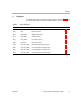
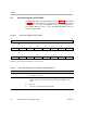
Table 6. Set Data Register (SET_DATA) Field Descriptions
Bit Field Value Description
31−16 Reserved 0 Reserved. The reserved bit location is always read as 0. A value written to
this field has no effect.
15−0 SETn Writing 1 sets the corresponding bit the OUT_DATA register. Reading this
register returns the contents of the OUT_DATA register. Writing a 0 has no
effect.
0 No effect
1 Sets the corresponding bit in OUT_DATA