
- TMS320C645x General-Purpose Input/Output SPRU724 User's Guide

Registers
General-Purpose Input/Output (GPIO)18 SPRU724
5.3 Output Data Register (OUT_DATA)
The GPIO output data register (OUT_DATA) indicates the value to be driven
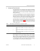
on a given GPIO output pin. The OUT_DATA registers are shown in Figure 5
and described in Table 5.
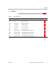
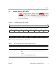
Figure 5. Output Data Register (OUT_DATA)
31 16
Reserved
R-0
15 14 13 12 11 10 9 8
OUT15
OUT14 OUT13 OUT12 OUT11 OUT10 OUT9 OUT8
R/W-0 R/W-0 R/W-0 R/W-0 R/W-0 R/W-0 R/W-0 R/W-0
76543210
OUT7 OUT6 OUT5 OUT4 OUT3 OUT2 OUT1 OUT0
R/W-0 R/W-0 R/W-0 R/W-0 R/W-0 R/W-0 R/W-0 R/W-0
Legend: R = Read only; R/W = Read/Write; -n = value after reset
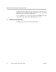
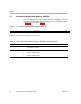
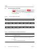
Table 5. Output Data Register (OUT_DATA) Field Descriptions
Bit Field Value Description
31−16 Reserved 0 Reserved. The reserved bit location is always read as 0. A value written to
this field has no effect.
15−0 OUTn Controls the drive state of the corresponding GPn pin. These bits do not
affect the state of the pin when the pin is configured as an input. Reading
these bits returns the value of this register, not the state of the pin.