TMS320C645x DSP General-Purpose Input/Output (GPIO) User’s Guide Literature Number: SPRU724 December 2005
IMPORTANT NOTICE Texas Instruments Incorporated and its subsidiaries (TI) reserve the right to make corrections, modifications, enhancements, improvements, and other changes to its products and services at any time and to discontinue any product or service without notice. Customers should obtain the latest relevant information before placing orders and should verify that such information is current and complete.
Preface Read This First About This Manual This document describes the general-purpose input/output (GPIO) peripheral in the digital signal processors (DSPs) of the TMS320C645x™ DSP family. Notational Conventions This document uses the following conventions. - Hexadecimal numbers are shown with the suffix h. For example, the following number is 40 hexadecimal (decimal 64): 40h.
Trademarks Related Documentation From Texas Instruments / Trademarks TMS320C6000 Programmer’s Guide (literature number SPRU198) describes ways to optimize C and assembly code for the TMS320C6000t DSPs and includes application program examples. TMS320C6000 Code Composer Studio Tutorial (literature number SPRU301) introduces the Code Composer Studiot integrated development environment and software tools.
Contents Contents 1 Overview . . . . . . . . . . . . . . . . . . . . . . . . . . . . . . . . . . . . . . . . . . . . . . . . . . . . . . . . . . . . . . . . . . . . . . . . . . 9 2 GPIO Function . . . . . . . . . . . . . . . . . . . . . . . . . . . . . . . . . . . . . . . . . . . . . . . . . . . . . . . . . . . . . . . . . . . 12 3 Interrupt and Event Generation . . . . . . . . . . . . . . . . . . . . . . . . . . . . . . . . . . . . . . . . . . . . . . . . . . . . 13 4 Emulation Halt Operation . . .
Figures Figures 1 2 3 4 5 6 7 8 9 10 11 12 6 TMS320C645x DSP Block Diagram . . . . . . . . . . . . . . . . . . . . . . . . . . . . . . . . . . . . . . . . . . . . . . GPIO Peripheral Block Diagram . . . . . . . . . . . . . . . . . . . . . . . . . . . . . . . . . . . . . . . . . . . . . . . . . . Interrupt Per-Bank Enable Register (BINTEN) . . . . . . . . . . . . . . . . . . . . . . . . . . . . . . . . . . . . . Direction Register (DIR) . . . . . . . . . . . . . . . . . . . . . . . . . . . . . . . . . . .
Tables Tables 1 2 3 4 5 6 7 8 9 10 11 12 GPIO Interrupt and EDMA Event Configuration Options . . . . . . . . . . . . . . . . . . . . . . . . . . . . . GPIO Registers . . . . . . . . . . . . . . . . . . . . . . . . . . . . . . . . . . . . . . . . . . . . . . . . . . . . . . . . . . . . . . . . Interrupt Per-Bank Enable Register (BINTEN) Field Descriptions . . . . . . . . . . . . . . . . . . . . . Direction Register (DIR) Field Descriptions . . . . . . . . . . . . . . . . . . . . . . . . . . . . . . . . . .
This page is intentionally left blank.
General-Purpose Input/Output (GPIO) This document describes the general-purpose input/output (GPIO) peripheral in the digital signal processors (DSPs) of the TMS320C645x™ DSP family. 1 Overview The general-purpose input/output (GPIO) peripheral provides dedicated general-purpose pins that can be configured as either inputs or outputs. When configured as an output, you can write to an internal register to control the state driven on the output pin.
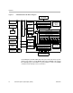
Overview Figure 1.
Overview Figure 2.
GPIO Function 2 GPIO Function You can independently configure each GPIO pin (GPn) as either an input or an output using the GPIO direction registers. The GPIO direction register (DIR) specifies the direction of each GPIO signal. Logic 0 indicates the GPIO pin is configured as output, and logic 1 indicates input. When configured as output, writing a 1 to a bit in the set data register drives the corresponding GPn to a logic-high state.
Interrupt and Event Generation 3 Interrupt and Event Generation Each GPIO pin (GPn) can be configured to generate a CPU interrupt (GPINTn) and a synchronization event to the EDMA controller (GPINTn). The interrupt and EDMA event can be generated on the rising-edge, falling-edge, or on both edges of the GPIO signal. The edge detection logic is synchronized to the GPIO peripheral clock. The direction of the GPIO pin does not need to be input when using the pin to generate the interrupt and EDMA event.
Emulation HaltEvent Operation Interrupt and Generation / Interrupts and Events Reading the SET_RIS_TRIG or CLR_RIS_TRIG register returns the value of RIS_TRIG register. Reading from SET_FAL_TRIG and CLR_FAL_TRIG register returns the value of FAL_TRIG register. To use the GPIO pins as sources for CPU interrupts and EDMA events, bit 0 in the bank interrupt enable register (BINTEN) must be set to 1. 4 Emulation Halt Operation The GPIO peripheral is not affected by emulation halts.
Registers 5 Registers The GPIO peripheral is configured through the registers listed in Table 2. See the device-specific datasheet for the memory address of these registers. Table 2. GPIO Registers Offsets Acronym Register Name 0008 BINTEN Interrupt Per-Bank Enable Register 5.1 0010 DIR Direction Register 5.2 0014 OUT_DATA Output Data Register 5.3 0018 SET_DATA Set Data Register 5.4 001C CLR_DATA Clear Data Register 5.5 0020 IN_DATA Input Data Register 5.
Registers 5.1 Interrupt Per-Bank Enable Register (BINTEN) To use the GPIO pins as sources for CPU interrupts and EDMA events, bit 0 in the bank interrupt enable register (BINTEN) must be set. BINTEN is shown in Figure 3 and described in Table 3. Figure 3. Interrupt Per-Bank Enable Register (BINTEN) 31 1 0 Reserved EN R-0 RW-0 Legend: R = Read only; R/W = Read/Write; -n = value after reset Table 3.
Registers 5.2 Direction Register (DIR) The GPIO direction register (DIR) determines if a given GPIO pin is an input or an output. The GPDIR is shown in Figure 4 and described in Table 4. By default, all the GPIO pins are configured as input pins. When GPIO pins are configured as output pins, the GPIO output buffer drives the GPIO pin. If it is necessary to place the GPIO output buffer in a high-impedance state, the GPIO pin must be configured as an input pin (DIRn = 0).
Registers 5.3 Output Data Register (OUT_DATA) The GPIO output data register (OUT_DATA) indicates the value to be driven on a given GPIO output pin. The OUT_DATA registers are shown in Figure 5 and described in Table 5. Figure 5.
Registers 5.4 Set Data Register (SET_DATA) The GPIO set data register (SET_DATA) is shown in Figure 6 and described in Table 6. SET_DATA provides an alternate means of driving GPIO outputs high. Writing a 1 to a bit of SET_DATA sets the corresponding bit in OUT_DATA. Writing a 0 has no effect. Reading SET_DATA returns the contents of OUT_DATA. Figure 6.
Registers 5.5 Clear Data Register (CLR_DATA) The GPIO clear data register (CLR_DATA) is shown in Figure 7 and described in Table 7. CLR_DATA provides an alternate means of driving GPIO outputs low. Writing a 1 to a bit of CLR_DATA clears the corresponding bit in OUT_DATA. Writing a 0 has no effect. Reading CLR_DATA returns the contents of OUT_DATA. Figure 7.
Registers 5.6 Input Data Register (IN_DATA) The GPIO input data register (IN_DATA) reflects the state of the GPIO pins. The IN_DATA register is shown in Figure 8 and described in Table 8. When read, IN_DATA returns the state of the GPIO pins regardless of the state of the corresponding bits in the DIR and OUT_DATA registers. Figure 8.
Registers 5.7 Set Rising Edge Interrupt Register (SET_RIS_TRIG) The GPIO rising trigger register (RIS_TRIG) configures the edge detection logic to trigger GPIO interrupts and EDMA events on the rising edge of GPIO signals. Setting a bit to 1 in RIS_TRIG causes the corresponding GPIO interrupt and EDMA event (GPINTn) to be generated on the rising edge of GPn. RIS_TRIG is not directly accessible by the CPU; it must be configured using the GPIO set rising trigger and clear rising trigger registers.
Registers 5.8 Clear Rising Edge Interrupt Register (CLR_RIS_TRIG) The GPIO rising trigger register (RIS_TRIG) configures the edge detection logic to trigger GPIO interrupts and EDMA events on the rising edge of GPIO signals. Setting a bit to 1 in RIS_TRIG causes the corresponding GPIO interrupt and EDMA event (GPINTn) to be generated on the rising edge of GPn. RIS_TRIG is not directly accessible by the CPU; it must be configured using the GPIO set rising trigger and clear rising trigger registers.
Registers 5.9 Set Falling Edge Interrupt Register (SET_FAL_TRIG) The GPIO falling trigger register (FAL_TRIG) configures the edge detection logic to trigger GPIO interrupts and EDMA events on the falling edge of GPIO signals. Setting a bit to 1 in FAL_TRIG causes the corresponding GPIO interrupt and EDMA event (GPINTn) to be generated on the falling edge of GPn. FAL_TRIG is not directly accessible by the CPU; it must be configured using the GPIO set falling trigger and clear falling trigger registers.
Registers 5.10 Clear Falling Edge Interrupt Register (CLR_FAL_TRIG) The GPIO falling trigger register (FAL_TRIG) configures the edge detection logic to trigger GPIO interrupts and EDMA events on the falling edge of GPIO signals. Setting a bit to 1 in FAL_TRIG causes the corresponding GPIO interrupt and EDMA event (GPINTn) to be generated on the falling edge of GPn. FAL_TRIG is not directly accessible by the CPU; it must be configured using the GPIO set falling trigger and clear falling trigger registers.
This page is intentionally left blank.
Index Index B I block diagram C645x DSP GPIO 11 interrupt generation interrupts 14 13 10 N notational conventions E O overview event generation events 3 14 9 13 R registers 15 related documentation from Texas Instruments F function 12 SPRU724 3 T trademarks 4 General-Purpose Input/Output (GPIO) 27