
User's Manual

6 Registers
www.ti.com
Registers
The TCP2 contains several memory-mapped registers accessible via the CPU, QDMA, and EDMA3. A
peripheral-bus access is faster than an EDMA3-bus access for isolated accesses (typically when
accessing control registers). EDMA3-bus accesses are intended to be used for EDMA3 transfers and are
meant to provide maximum throughput to/from the TCP2.
The memory map is listed in Table 3 , including all TCP2 memories (systematic and parity, interleaver,
hard decisions, a priori, and extrinsic). All addresses provided are offset addresses. For the TCP2 base
data address and TCP2 base control address, see the device-specific data manual.
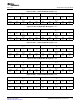
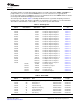
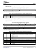
Table 3. TCP2 Registers
TCP2 Data Offset TCP2 Control Register/Memory
Address Offset Address Abbreviation Name See
0x00000 TCPPID TCP Peripheral Identification Register Section 6.1
0x00000 TCPIC0 TCP Input Configuration Register 0 Section 6.2
0x00004 TCPIC1 TCP Input Configuration Register 1 Section 6.3
0x00008 TCPIC2 TCP Input Configuration Register 2 Section 6.4
0x0000C TCPIC3 TCP Input Configuration Register 3 Section 6.5
0x00010 TCPIC4 TCP Input Configuration Register 4 Section 6.6
0x00014 TCPIC5 TCP Input Configuration Register 5 Section 6.7
0x00018 TCPIC6 TCP Input Configuration Register 6 Section 6.8
0x0001C TCPIC7 TCP Input Configuration Register 7 Section 6.10
0x00020 TCPIC8 TCP Input Configuration Register 8 Section 6.11
0x00024 TCPIC9 TCP Input Configuration Register 9 Section 6.12
0x00028 TCPIC10 TCP Input Configuration Register 10 Section 6.13
0x0002C TCPIC11 TCP Input Configuration Register 11 Section 6.14
0x00030 TCPIC12 TCP Input Configuration Register 12 Section 6.15
0x00034 TCPIC13 TCP Input Configuration Register 13 Section 6.16
0x00038 TCPIC14 TCP Input Configuration Register 14 Section 6.17
0x0003C TCPIC15 TCP Input Configuration Register 15 Section 6.18
0x00040 TCPOUT0 TCP Output Parameters Register 0 Section 6.19
0x00044 TCPOUT1 TCP Output Parameters Register 1 Section 6.20
0x00048 TCPOUT2 TCP Output Parameters Register 2 Section 6.21
0x0004C TCPEXE TCP Execute Register Section 6.22
0x00050 TCPEND TCP Endianness Register Section 6.23
0x00060 TCPERR TCP Error Register Section 6.24
0x00068 TCPSTAT TCP Status Register Section 6.25
0x00070 TCPEMU TCP Emulation Register Section 6.26
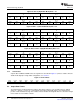
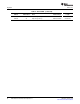
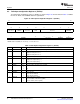
Table 4. TCP2 RAMs
TCP2 Data Offset Register/Memory
Address Abbreviation Name Address Range Length
0x10000 X0 Data/Sys and Parity Memory 0x10000-0x243FF 0x00014400
0x30000 W0 Extrinsic Mem 0 0x30000-0x351FF 0x00005100
0x40000 W1 Extrinsic Mem 1 0x40000-0x451FF 0x00005100
0x50000 I0 Interleaver Memory 0x50000-0x5a1FF 0x0000A200
0x60000 O0 Output/Decision Memory 0x60000-0x60a7F 0x00000A20
0x70000 S0 Scratch Pad Memory 0x70000-0x70aFF 0x000006E0
0x80000 T0 Beta State Memory 0x80000-0x80FFF 0x00000A00
0x90000 C0 CRC Memory 0x90000-0x90FFF 0x000001C0
SPRUGK1 – March 2009 TMS320C6457 Turbo-Decoder Coprocessor 2 25
Submit Documentation Feedback