
Network Router User Manual


www.ti.com
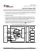
Introduction to the HPI
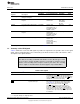
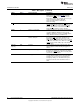
Table 1. Summary of HPI Registers
Host Access CPU Access
Read/Write Access Requirements Read/Write Offset
Register Description Permissions Permissions Address
PWREMU_MGMT Power and Emulation None - Read/Write 04h
Management Register
HPIC Host Port Interface Control Read/Write HCNTL1 low Read: All bits 30h
Register HCNTL0 low Write: HINT
and DSPINT
bits only
HPIAW Host Port Interface Write Address Read/Write HCNTL1 high Read only 34h
Register HCNTL0 low
Single-HPIA mode, or
dual-HPIA mode with
HPIAW selected
(1)
HPIAR Host Port Interface Read Address Read/Write HCNTL1 high Read only 38h
Register HCNTL0 low
Single-HPIA mode, or
dual-HPIA mode with
HPIAR selected
(1)
HPID Host Port Interface Data Register Read/Write With autoincrementing: None None
HCNTL1 low
HCNTL0 high
No autoincrementing:
HCNTL1 high
HCNTL0 high
(1)
The single-HPIA mode and the dual-HPIA mode are described in Section 2.
1.2 Summary of the HPI Signals
Table 2 summarizes each of the HPI signals. It provides the signal name, the possible states for the signal
(input, output, or high-impedance), the connection(s) to be made on the host side of the interface, and a
description of the signal’s function.
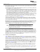
CAUTION
Note that the encoding of HCNTL0 and HCNTL1 for the different types of HPI
accesses varies on many TI DSPs; therefore, you should use caution to ensure
that the correct encoding of these inputs is used for your device. The encoding
of these signals as described in this document applies only to C6457 DSPs.
Table 2. HPI Signals
Signal State
(1)
Host Connection Description
HCS I Chip select pin HPI chip select. HCS must be low for the HPI to be
selected by the host. HCS can be kept low between
accesses. HCS normally precedes an active HDS (data
strobe) signal, but can be connected to an HDS pin for
simultaneous select and strobe activity.
HDS1 and I Read strobe and write strobe pins or HPI data strobe pins. These pins are used for strobing
HDS2 any data strobe pin data in and out of the HPI (for data strobing details,
see Section 3.3). The direction of the data transfer
depends on the logic level of the HR/W signal.
The HDS signals are also used to latch control
information (if HAS is tied high) on the falling edge.
During an HPID write access, data is latched into the
HPID register on the rising edge of HDS. During read
operations, these pins act as output-enable pins of the
host data bus.
(1)
I = Input, O = Output, Z = High Impedance.
9
SPRUGK7A–March 2009–Revised July 2010 Host Port Interface (HPI)
Copyright © 2009–2010, Texas Instruments Incorporated